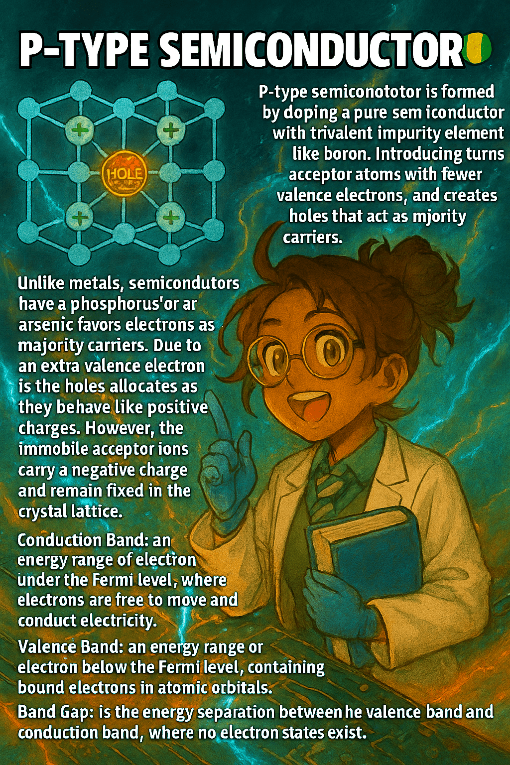
A p-type semiconductor is formed by doping a pure semiconductor, such as silicon, with trivalent elements like boron, gallium, or indium.
These dopants have only three valence electrons, one fewer than silicon, which creates a vacancy or “hole” in the crystal lattice.
Holes act as positive charge carriers because electrons from neighboring atoms can move to fill them, effectively shifting the vacancy through the lattice.
In p-type materials, holes are the majority carriers, while electrons are the minority carriers.
This unique property allows p-type semiconductors to complement n-type semiconductors in forming p–n junctions, which are the basis of diodes, transistors, and solar cells.
The interaction between electrons and holes in these junctions enables rectification, amplification, and energy conversion.
P-type semiconductors are therefore critical in designing circuits that control and manipulate electrical signals, forming the foundation of countless electronic devices.
BitcoinVersus.Tech Editor’s Note:
We volunteer daily to ensure the credibility of the information on this platform is Verifiably True.
If you would like to support to help further secure the integrity of our research initiatives, please donate here: bc1qrved9tfquym6u3age7xhmnkjs2lq8j9aulperagkuhtuk5w5c35ssfpge8
BitcoinVersus.tech is not a financial advisor. This media platform reports on financial subjects purely for informational purposes

Leave a comment