Flatband capacitance is a central concept in metal oxide semiconductor physics and is used to evaluate how a device behaves when no electric field exists inside the semiconductor.
It represents the capacitance of a metal oxide semiconductor structure at the point where the semiconductor energy bands are perfectly flat.
When the bands are flat, the applied voltage has canceled out the natural work function difference between the gate material and the semiconductor, so the semiconductor contains no depletion charge, no inversion charge, and no internal electric field.
Under these conditions the semiconductor acts like a simple dielectric material, and the total capacitance is determined mainly by the oxide capacitance together with the geometric contribution of the semiconductor itself.
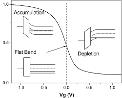
The image illustrates the typical high-frequency Capacitance-Voltage (C-V) curve for an ideal Metal-Oxide-Semiconductor (MOS) capacitor built on a p-type semiconductor substrate, demonstrating the three main operational modes. On the vertical axis, the capacitance is normalized by the maximum oxide capacitance (1.0 equals Cox), and the horizontal axis represents the gate voltage (Vg). The curve begins in the Accumulation region at negative voltages (e.g., Vg=−1.0V), where the capacitance is high and near Cox, indicating holes are concentrated at the semiconductor-oxide interface, causing the energy bands to bend sharply upwards. As the voltage approaches zero, the structure enters the Flat Band condition at Vg=0V, where the energy bands are level, the surface potential is zero, and the capacitance hits the specific Flat-Band Capacitance (CFB) value. Moving into positive voltages (e.g., Vg=0.5V), the device enters the Depletion region, causing the energy bands to bend downwards and the capacitance to drop rapidly as a space-charge region is formed in the semiconductor. Image credit: Reasearchgate.net.
Flatband capacitance is extremely important because it provides a reference point for extracting oxide thickness, evaluating interface traps, identifying fixed charges in the oxide, and confirming the quality of the oxide semiconductor boundary.
In capacitance voltage measurements, the location of flatband capacitance reveals how clean or distorted the device fabrication process was and can show whether impurities or charge shifts are present.
Engineers rely on flatband capacitance to verify material uniformity, confirm correct doping models, and diagnose problems that can affect threshold voltage stability and long term device reliability. It is one of the key parameters used to judge the electrical integrity of semiconductor devices and supports accurate modeling from research labs to advanced transistor manufacturing.
BitcoinVersus.Tech Editor’s Note:
We volunteer daily to ensure the credibility of the information on this platform is Verifiably True.
If you would like to support to help further secure the integrity of our research initiatives, please donate here: bc1qrved9tfquym6u3age7xhmnkjs2lq8j9aulperagkuhtuk5w5c35ssfpge8
BitcoinVersus.tech is not a financial advisor. This media platform reports on financial subjects purely for informational purposes.

Leave a comment