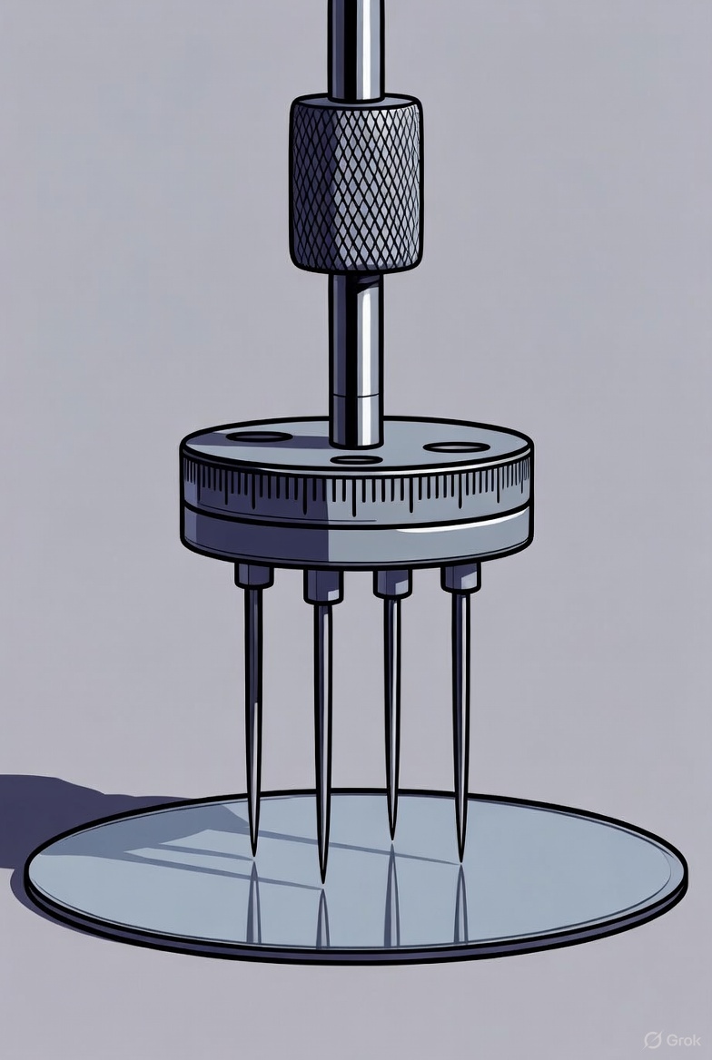
The Four-Point Probe (4PP) method is a standard, non-destructive technique used in semiconductor manufacturing and research to accurately measure the sheet resistance and subsequent resistivity of thin films, wafers, and other semiconductor materials.
This technique uses a linear array of four closely spaced, collinear probes typically made of tungsten or beryllium copper, each mounted on springs to ensure good contact with the material surface.
Unlike the simpler two-point probe method, the 4PP method effectively eliminates the error introduced by contact resistance—the unwanted resistance generated at the interface between the metal probe and the semiconductor surface.
A precisely known DC current (I) is passed between the two outer probes, while the resulting voltage drop ($V$) is simultaneously measured by a high-impedance voltmeter between the two inner probes.
By spatially separating the current injection and voltage sensing paths, the method ensures that the voltage measurement is solely dependent on the material’s properties and not the fluctuating contact resistances.
The sheet resistance is then calculated directly from the measured voltage and current using a formula that incorporates geometric correction factors specific to the probe spacing and sample size.
This makes the 4PP method indispensable for quality control and process monitoring in integrated circuit fabrication.
BitcoinVersus.Tech Editor’s Note:
We volunteer daily to ensure the credibility of the information on this platform is Verifiably True.
If you would like to support to help further secure the integrity of our research initiatives, please donate here: bc1qrved9tfquym6u3age7xhmnkjs2lq8j9aulperagkuhtuk5w5c35ssfpge8
BitcoinVersus.tech is not a financial advisor. This media platform reports on financial subjects purely for informational purposes.

Leave a comment