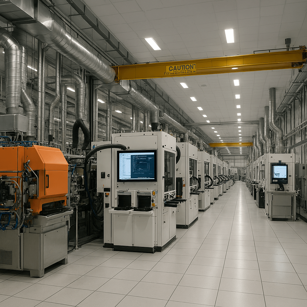
Semiconductor packaging is the stage where a bare chip is turned into a usable component that can safely live on a circuit board and inside a product.
In simple terms, packaging encloses one or more semiconductor dies in a protective structure made of plastic, ceramic, glass, or metal, adds the external pins or balls that connect it to a circuit board, and helps carry heat away from the chip.
Before packaging, devices exist only as tiny dies on a wafer and cannot be handled or connected reliably. Packaging transforms those fragile dies into standardized parts like QFN, BGA, or chip scale packages that can be assembled on printed circuit boards at scale.
The package has three main jobs. It protects the silicon from the environment by blocking moisture, contaminants, and mechanical stress that would quickly degrade exposed circuitry.
It creates electrical connections between microscopic bond pads on the die and the outside world using structures such as wire bonds, bumps, or copper posts, which then connect to leads, lands, or balls on the package surface that can be soldered to a board.
It also manages heat flow from the chip into the surrounding system through thermal paths, heat spreaders, or metal bodies so that the device can operate at its rated performance and lifetime. Because of these functions, the choice of materials and package design strongly affects reliability, signal integrity, and allowable power levels.
In the past, packaging was seen mainly as a protective shell around a single integrated circuit. Today it is a strategic part of the semiconductor stack.
Advanced semiconductor packaging combines multiple dies such as logic, memory, and analog or RF devices into a single module, using approaches like 2.5D interposers, 3D stacking, fan out wafer level packaging, and system in package.
This allows manufacturers to increase performance and bandwidth, reduce power consumption, and shrink board area without always needing a smaller process node. As a result, packaging has become a key way to extend Moore style scaling when transistor shrinks alone are more expensive or harder to achieve.
The importance of packaging in the industry is visible in national policy and corporate investment. Packaging influences power, performance, and cost at a system level, and packaging capacity is now viewed as a critical link in the chip supply chain for applications such as artificial intelligence accelerators and high bandwidth memory.
Governments are funding domestic advanced packaging facilities, and companies are building large dedicated packaging campuses to support leading edge wafer output. At the product level, new packaging innovations such as denser interconnect structures or improved substrates directly enable thinner consumer devices, better thermal behavior, and more compact high performance systems. In short, semiconductor packaging has moved from being an afterthought to being one of the core levers that determine how far the industry can push computing performance, efficiency, and integration.
BitcoinVersus.Tech Editor’s Note:
We volunteer daily to ensure the credibility of the information on this platform is Verifiably True.
If you would like to support to help further secure the integrity of our research initiatives, please donate here: bc1qrved9tfquym6u3age7xhmnkjs2lq8j9aulperagkuhtuk5w5c35ssfpge8
BitcoinVersus.tech is not a financial advisor. This media platform reports on financial subjects purely for informational purposes.

Leave a comment