Photoluminescence is a fundamental optical process in which a material emits light after absorbing photons, typically at a longer wavelength than the excitation source. When light of sufficient energy strikes a material, electrons are promoted from lower-energy states (often the valence band) to higher-energy states (such as the conduction band).
As these electrons relax back down, they release energy in the form of emitted photons. This emission provides a direct window into the material’s electronic structure, revealing properties such as band gap, defect states, and surface interactions.
The phenomenon can be divided into two main categories: fluorescence and phosphorescence. Fluorescence occurs almost instantaneously, with emission lifetimes on the order of nanoseconds to microseconds, and ceases once the excitation source is removed.
Phosphorescence, on the other hand, involves electrons trapped in metastable states, leading to delayed emission that can last from microseconds to seconds or even longer.
These differences make photoluminescence a versatile probe for studying both fast and slow electronic processes in materials.
Applications of photoluminescence span across multiple scientific and technological fields. In semiconductor physics, it is used to measure band gaps, assess doping levels, and detect defects in thin films and nanostructures.
In nanotechnology, quantum dots and other nanoscale materials are characterized by their unique photoluminescent signatures. In biology and medicine, fluorescent markers enable imaging of biomolecules and tissues with high sensitivity. Because photoluminescence is non-destructive and highly sensitive, it has become a cornerstone technique for material characterization, device development, and even environmental sensing.
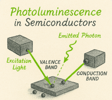
Photoluminescence in semiconductors refers to the emission of light that occurs when electrons and holes recombine after the semiconductor absorbs photons. When a semiconductor is illuminated with light of sufficient energy, electrons are excited from the valence band into the conduction band, leaving behind holes. These excited carriers can then relax back to lower energy states, and during recombination, photons are emitted. The wavelength (or energy) of this emitted light corresponds directly to the semiconductor’s band gap or to defect-related states within the material.
In practice, photoluminescence spectroscopy is a powerful, non-destructive tool for probing semiconductor properties. It can reveal the band gap energy, identify impurities or defects, measure carrier lifetimes, and assess the quality of thin films or nanostructures. For example, in direct band gap semiconductors like GaAs, strong photoluminescence signals are observed, while indirect band gap materials like silicon show weaker emission. This makes PL especially useful in research and industry for evaluating optoelectronic materials such as LEDs, solar cells, and laser diodes.
Furthermore, photoluminescence provides insight into nanoscale phenomena in advanced semiconductor structures. Quantum wells, quantum dots, and other nanostructures exhibit unique PL signatures due to quantum confinement effects, where the emission energy shifts depending on particle size. By analyzing these spectra, scientists can tailor semiconductor properties for specific applications, from high-efficiency photovoltaics to quantum communication devices.
BitcoinVersus.Tech Editor’s Note:
We volunteer daily to ensure the credibility of the information on this platform is Verifiably True.
If you would like to support to help further secure the integrity of our research initiatives, please donate here: bc1q5qgtq8szqa6yy38tqpsyuk3hynq8zy3xvqhsvzecj8lnryrnzhmqsfmwhh

Leave a comment