electrical engineering
-
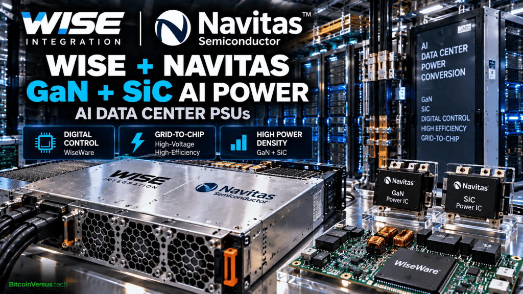
Wise Integration and Navitas Semiconductor are combining WiseWare digital control with GaN and SiC power semiconductors for AI data-center PSUs and grid-to-chip conversion.
-
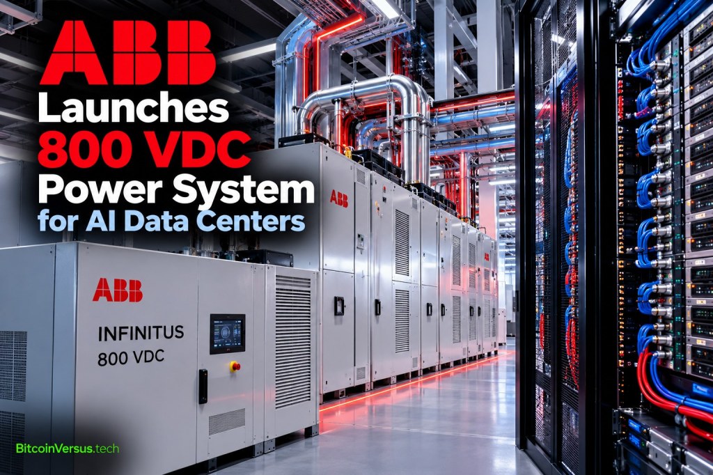
ABB’s new Infinitus portfolio moves AI data-center power toward source-to-rack 800 VDC with solid-state transformers, DC distribution, protection and cooling optimization.
-
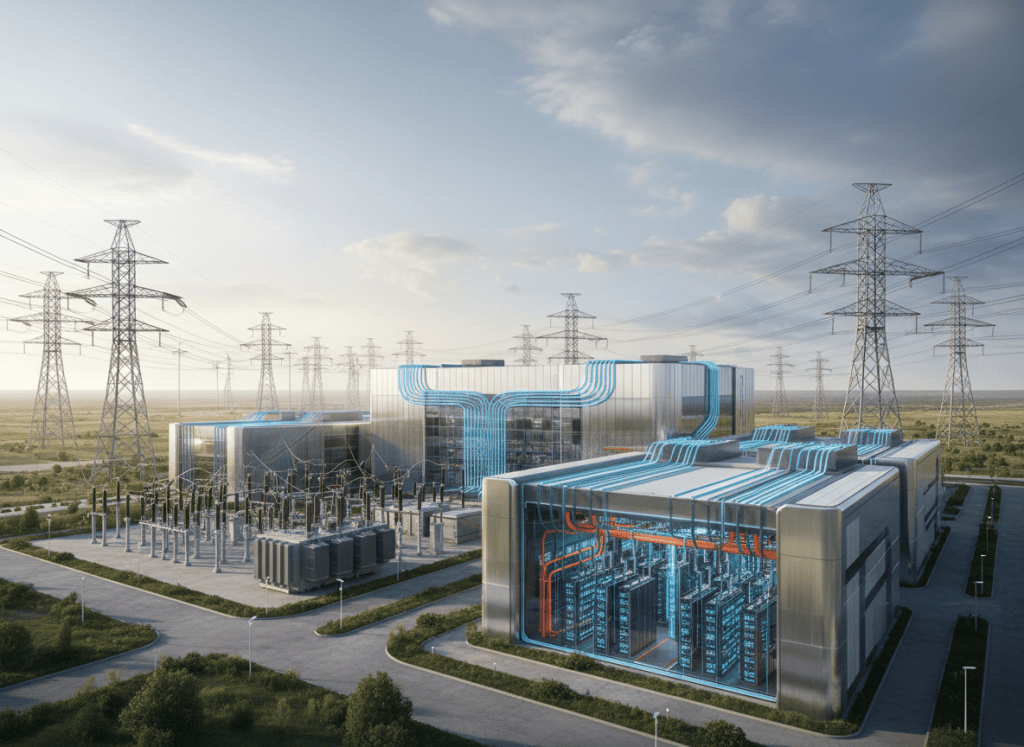
Huawei’s Grid-Interactive AIDC 1.0 combines 800 VDC-ready power, grid-forming energy storage and AI-powered liquid cooling for hyperscale AI infrastructure.
-
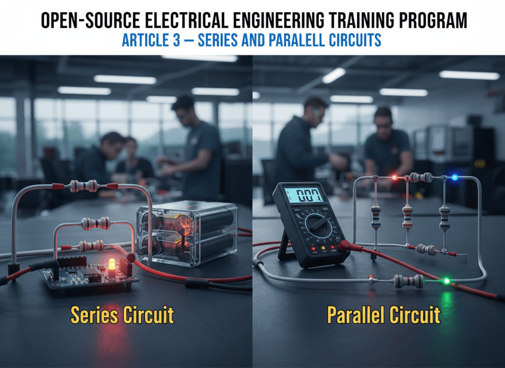
Article 3 explains series and parallel circuits, equivalent resistance, voltage and current relationships, and practical field applications.
-
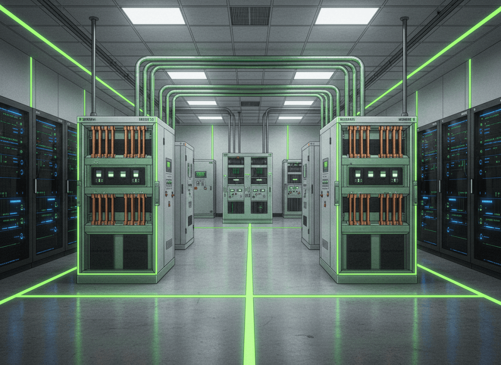
Eaton agreed to acquire Italy’s COL Group for €810 million, expanding European medium-voltage manufacturing for data centers and utilities.
-
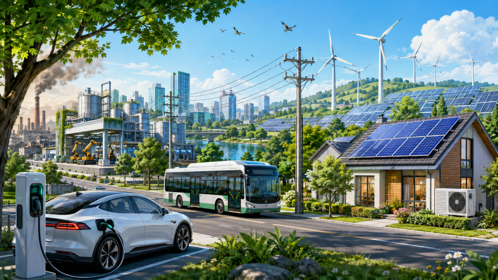
Electrification is the process of replacing technologies that directly burn gasoline, diesel, natural gas, or other fossil fuels with equipment powered by electricity. Common examples include replacing combustion vehicles with electric vehicles, gas furnaces with heat pumps, and fuel-powered industrial machinery with electric systems. When paired with renewable energy, nuclear power, energy storage, and a…
-
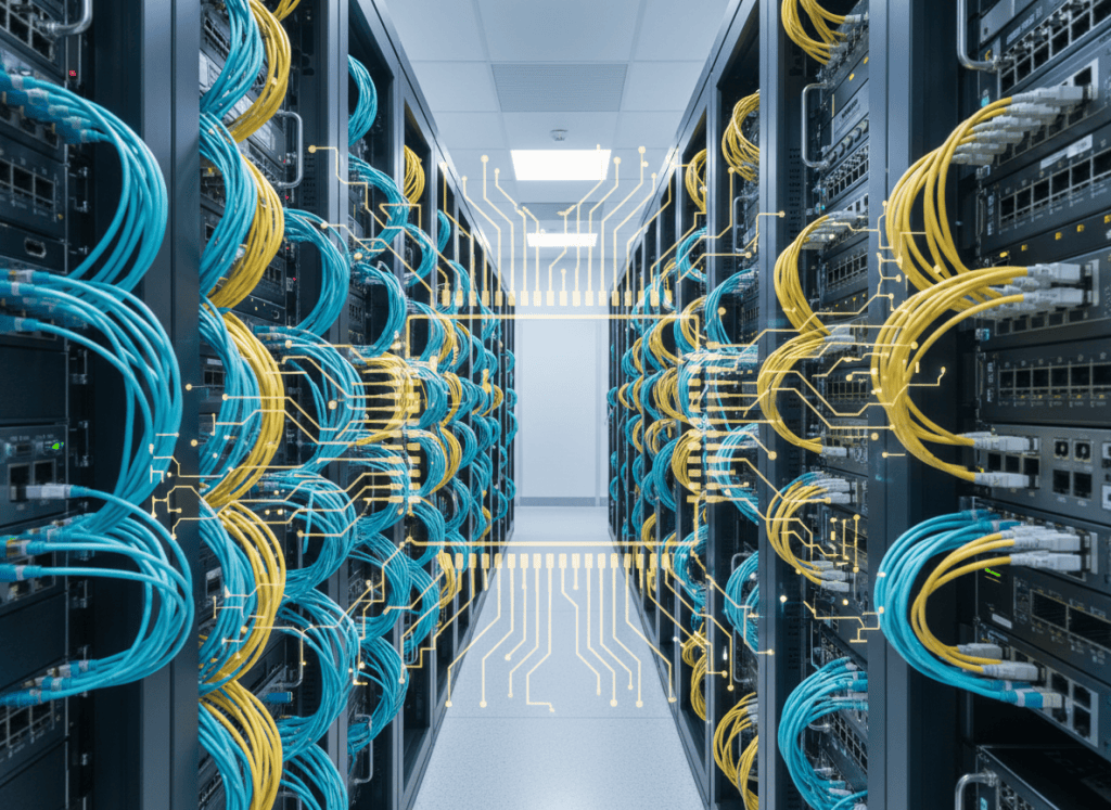
UL Solutions launched a manufacturer-focused certification program for medium-voltage solid-state power units that can support direct medium-voltage-to-800 VDC power delivery in AI data centers.
-
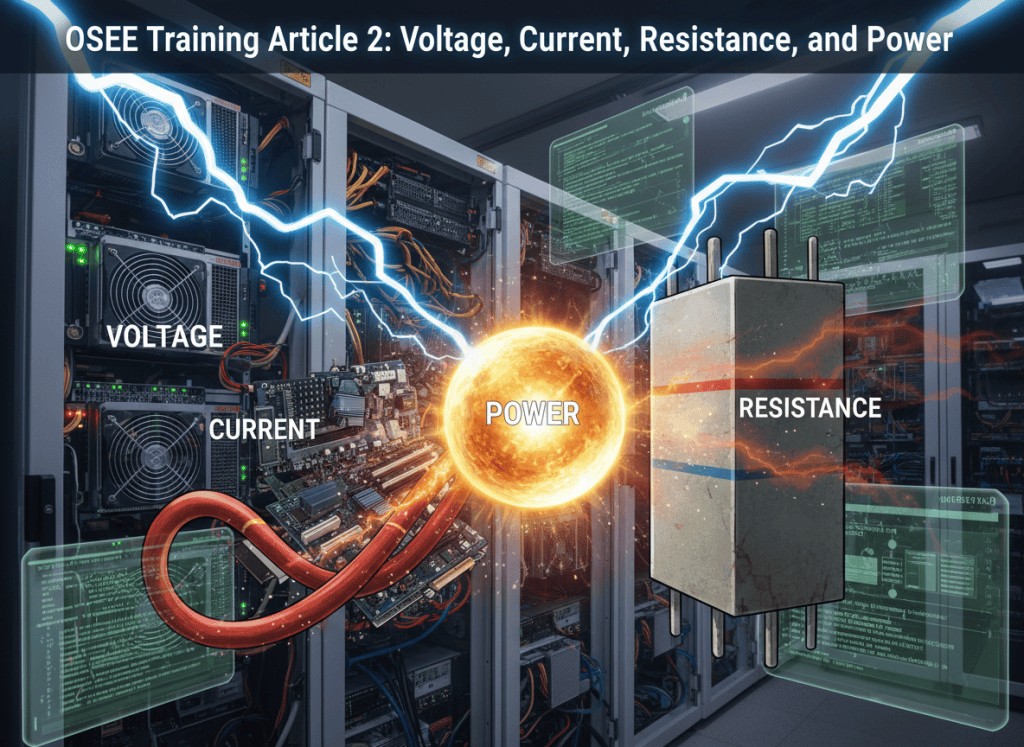
Article 2 introduces voltage, current, resistance, Ohm’s law, and electrical power as the foundation for later field and data-center electrical training.
-
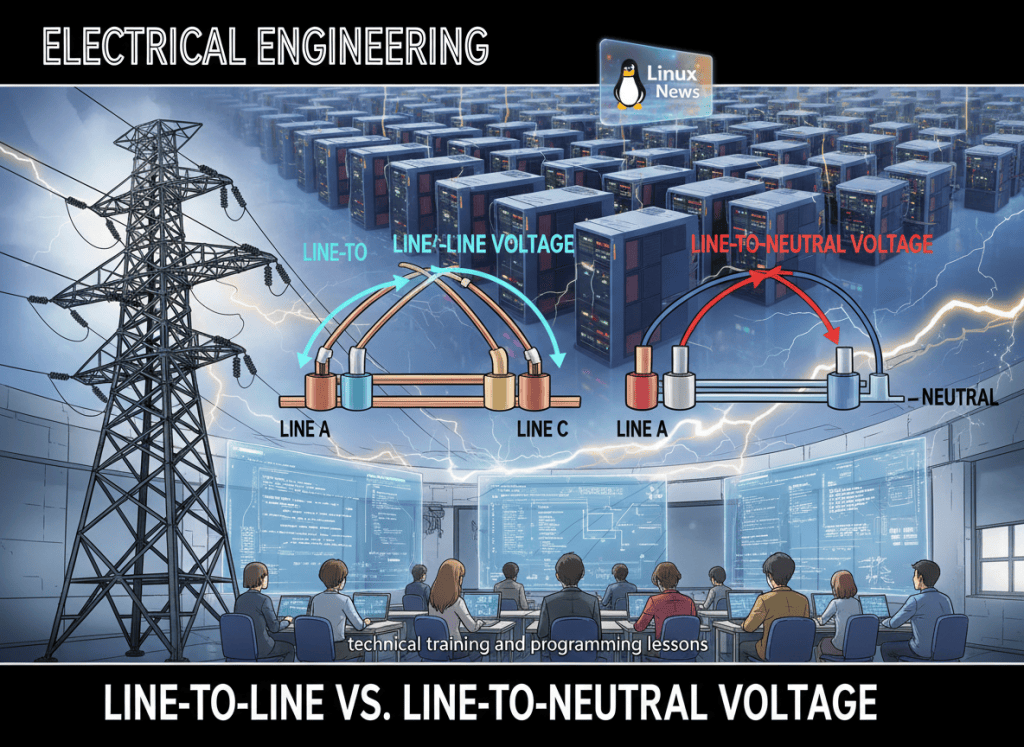
A practical guide to line-to-line and line-to-neutral voltage in 208Y/120 V and 480Y/277 V three-phase systems.
-
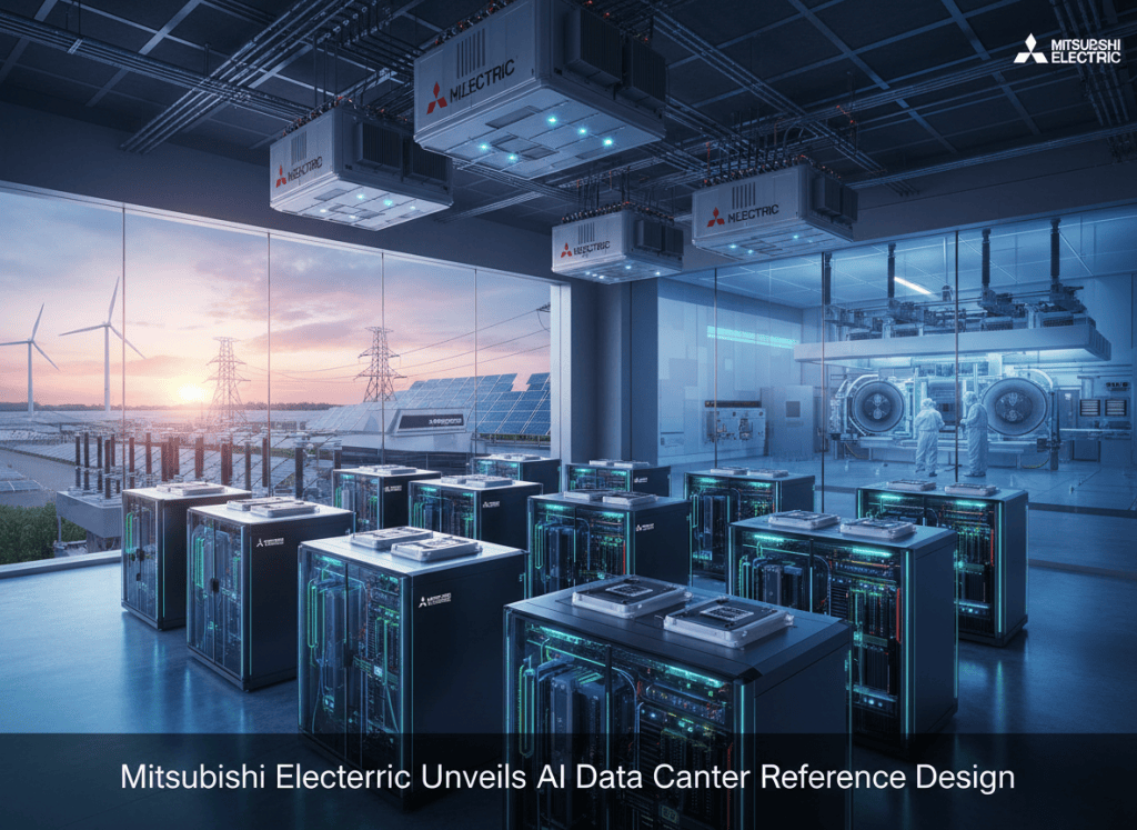
Mitsubishi Electric’s new NVIDIA-compatible AI data center reference design integrates 800 VDC power, on-site generation, battery storage, microgrids and dual-loop cooling for Vera Rubin infrastructure.
-
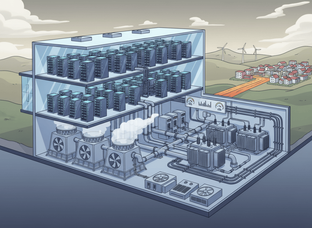
The European Commission has proposed a common sustainability rating system for large data centers as Europe prepares for rapid growth in artificial intelligence infrastructure. Facilities with installed information technology capacity of at least 500 kW already report operational data under EU energy efficiency rules, and the proposed rating system will turn reported information into comparable…
-
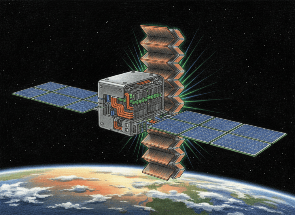
Starcloud plans to put Bitcoin-mining ASICs aboard an orbital data-center spacecraft, testing whether solar power can outweigh the challenges of cooling, launch cost and hardware reliability.

