semiconductors
-

A lattice atom refers to an atom that occupies a regular, repeating position within the crystal lattice of a solid material. In crystalline solids, atoms are arranged in a highly ordered structure known as a lattice, where each atom is situated at a specific point defined by the geometry of the unit cell. These lattice…
-
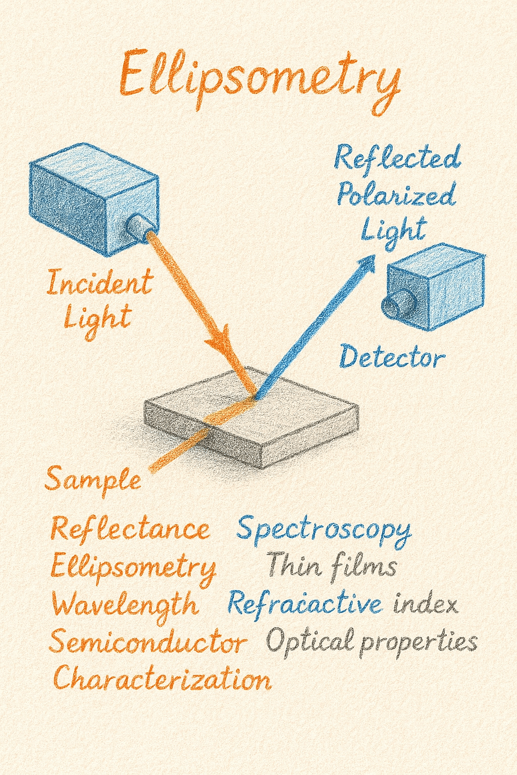
Ellipsometry is an advanced optical technique used to characterize thin films and surfaces by analyzing changes in the polarization of light upon reflection or transmission. In practice, a beam of polarized light is directed at a material, and the reflected or transmitted light undergoes a change in polarization that is measured as two parameters: the…
-

Solar cell roughness characterization is the process of analyzing and quantifying the surface texture of photovoltaic materials to understand how microscopic topographical features influence optical and electrical performance. The surface of a solar cell—whether crystalline silicon, thin-film, or emerging materials like perovskites—plays a critical role in determining how light interacts with the device. Controlled roughness…
-
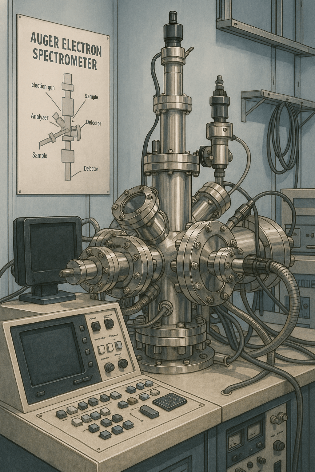
Auger Electron Spectroscopy (AES) is a powerful surface-sensitive analytical technique widely used in materials science to investigate the elemental composition of the outermost atomic layers of a sample. Unlike bulk characterization methods, AES focuses specifically on the top few nanometers of a material, making it invaluable for studying thin films, coatings, and surface modifications. The…
-

Polycrystalline silicon, often called poly-si, is a special material used to build the tiny pathways inside computer chips. Its main job is to control the flow of electricity, and a key property it has is called resistance. Resistance is how much a material slows down or fights against the electric current. Think of it like trying…
-

The solar energy industry traces its roots to nineteenth century scientific discoveries, beginning with the photovoltaic effect identified by Edmond Becquerel in 1839 and early selenium based cells in the late 1800s. It did not become a modern commercial sector until Bell Labs created the first practical silicon solar cell in 1954, which initially found…
-

Electron beam characterization involves using a focused beam of electrons to probe and analyze materials at very fine scales. Techniques such as scanning electron microscopy (SEM) and transmission electron microscopy (TEM) rely on the interaction between electrons and the atoms in a sample to reveal details about surface morphology, internal structure, and even chemical composition.…
-
The source‑series resistance (Rₛ) and drain‑series resistance (Rᴅ) are the parasitic resistances that appear in series with the source and drain terminals of a MOSFET. They arise from the silicon substrate, metallization layers, and package leads that connect the internal transistor to the external pins. When the device is turned on, the total on‑resistance (Rₒₙ)…
-
MOSFETs, or Metal-Oxide-Semiconductor Field-Effect Transistors, are essential components in modern electronics, and understanding their operating characteristics is crucial for anyone interested in electronics. These devices function as switches or amplifiers, controlling the flow of electrical current. The key to their operation lies in the voltage applied to the gate terminal, which influences the conductivity between…
-

Understanding oxide charge density in semiconductors is an important concept in electronics and materials science. Semiconductors are materials that have electrical properties between those of conductors and insulators. They are essential for making electronic devices like computers and smartphones. The oxide charge density refers to the amount of electric charge that is stored in the…
-

The flatband capacitance (CFB) is defined as the total measured capacitance of a Metal-Oxide-Semiconductor (MOS) structure or a similar semiconductor device when the applied gate voltage is exactly equal to the flatband voltage VFB. This flatband voltage represents the specific potential needed to establish the flatband condition, where the energy bands within the semiconductor substrate…
-

Metal oxide semiconductor capacitance voltage measurement is a way to electrically study what is happening at the surface of a semiconductor under a gate. The structure used is a simple capacitor made of a metal gate on top, a very thin insulating oxide in the middle, and a semiconductor such as silicon on the bottom.…
-

Instruction set architectures (ISAs) are crucial components of computer systems that define how software communicates with hardware. They specify the set of instructions that a processor can execute, including operations like arithmetic, data movement, and control flow. By establishing a standard interface, ISAs allow programmers to write software that can run on different hardware platforms…
-

Semiconductor packaging is the stage where a bare chip is turned into a usable component that can safely live on a circuit board and inside a product. In simple terms, packaging encloses one or more semiconductor dies in a protective structure made of plastic, ceramic, glass, or metal, adds the external pins or balls that…
-
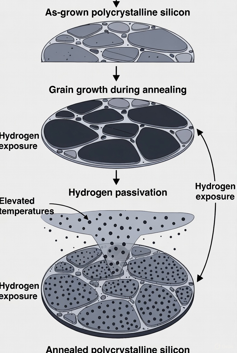
The annealing process in semiconductors is a crucial step in the manufacturing of electronic devices. This process involves heating the semiconductor material to a specific temperature and then allowing it to cool down slowly. The main purpose of annealing is to repair defects in the crystal structure of the semiconductor, which can occur during earlier…
-
The current flowing through a p-n junction diode (our one-way gate for electricity) is primarily controlled by four interacting factors. The most immediate control is the voltage applied across the diode: once the push from the battery reaches a certain minimum strength (the turn-on voltage), the current flow explodes exponentially, meaning a very small increase…
-

Forward bias is the electrical condition applied to a semiconductor diode to allow significant current to flow through it. This is achieved by connecting an external voltage source across the diode with the correct polarity: the positive terminal of the battery is connected to the diode’s P-type semiconductor (the anode), and the negative terminal is connected…
-
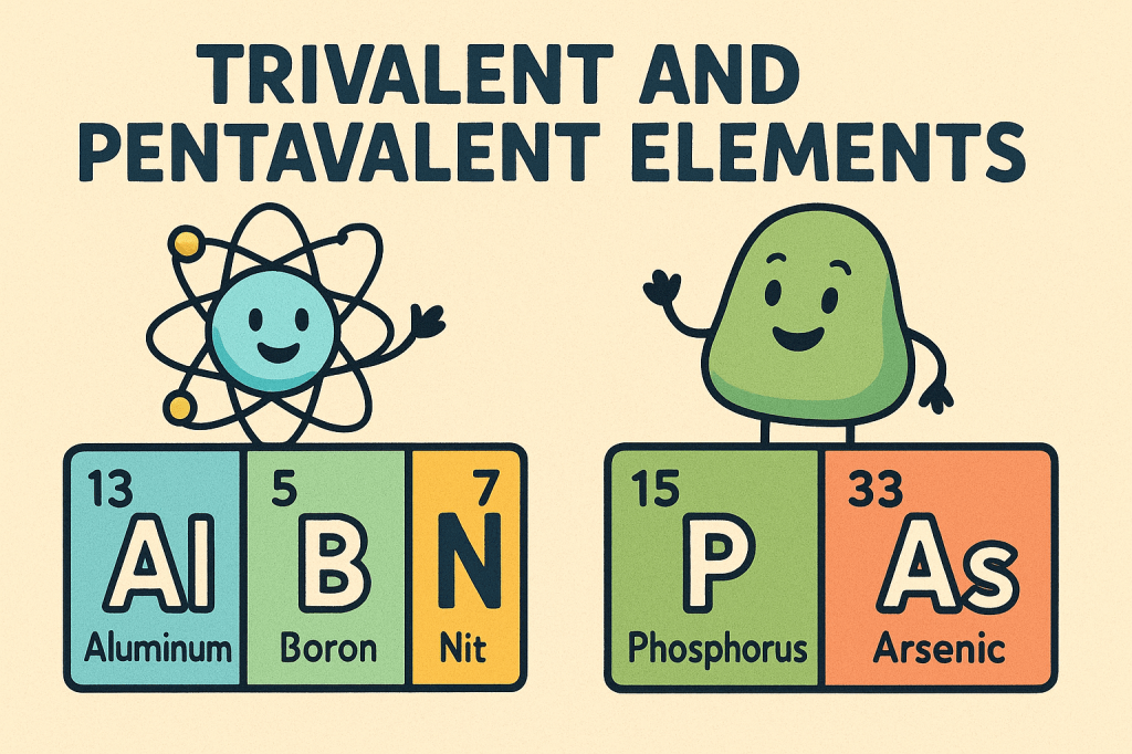
Trivalent and pentavalent elements are terms used to describe the number of valence electrons that an atom has available for bonding. Trivalent elements have three valence electrons, which means they can form three bonds with other atoms. This property is often seen in elements like aluminum and gallium. These elements typically participate in chemical reactions…
-
The ideality factor in diodes is a crucial concept that helps us understand how well a diode performs compared to an ideal diode. An ideal diode is a perfect device that allows current to flow in one direction without any resistance or loss of energy. However, real diodes are not perfect; they have some limitations…
-
When we talk about diode series resistance, we are referring to the resistance that is present in the diode when it is conducting current. This resistance is not just a simple number; it can change based on various factors, such as the amount of current flowing through the diode and the temperature of the diode…
-

Photovoltaics is the technological principle and scientific field concerned with the direct conversion of light energy, specifically photons from sunlight, into electrical energy through the photovoltaic effect, a physical and chemical process that occurs within a class of materials known as semiconductors, most commonly crystalline silicon. The fundamental unit of this conversion is the photovoltaic cell,…
-
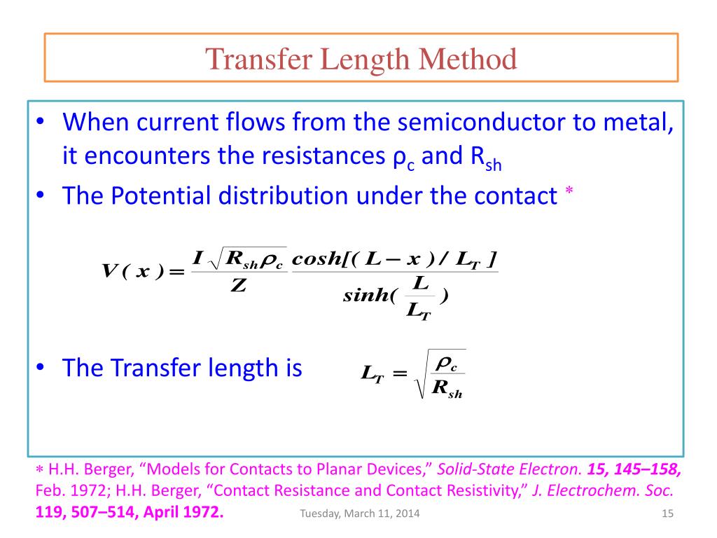
The Transfer Length Method (TLM) is a widely used technique in semiconductor physics and engineering for determining the specific contact resistivity between a metal and a semiconductor. It was developed as a response to the increasing significance of contact resistance in microelectronic devices due to device miniaturization. In practice, TLM involves depositing a series of…
-
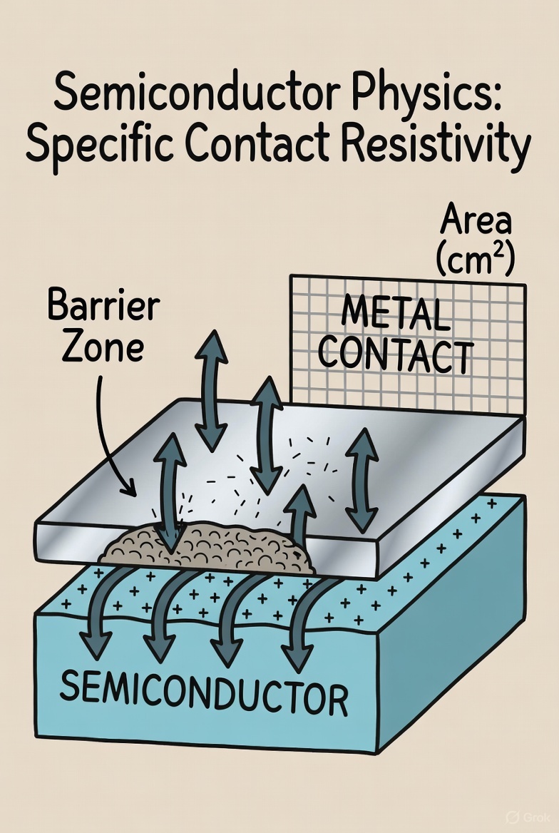
Specific contact resistivity is the fundamental measure of how effectively a metal makes an electrical connection to a semiconductor material. Think of it as a report card for the quality of the contact itself, completely separate from its physical size. Its value, given in units of Ohm-centimeters squared, tells you how much inherent resistance exists…
-

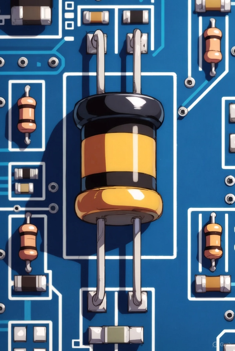
Contact resistance in semiconductor diodes refers to the parasitic electrical resistance that arises at the interfaces between the semiconductor material and the metal contacts (electrodes) that are attached to it. These metal-semiconductor interfaces are critical for injecting current into or extracting current from the active regions of the diode. The origin of this resistance is…
-
Resistance is the measurable opposition to the flow of electric current presented by a specific, complete object, such as a wire or a resistor. It is an extrinsic property, meaning its value is not fixed but is instead dictated by the physical geometry of the object. A long and narrow component will exhibit high resistance, making…
-
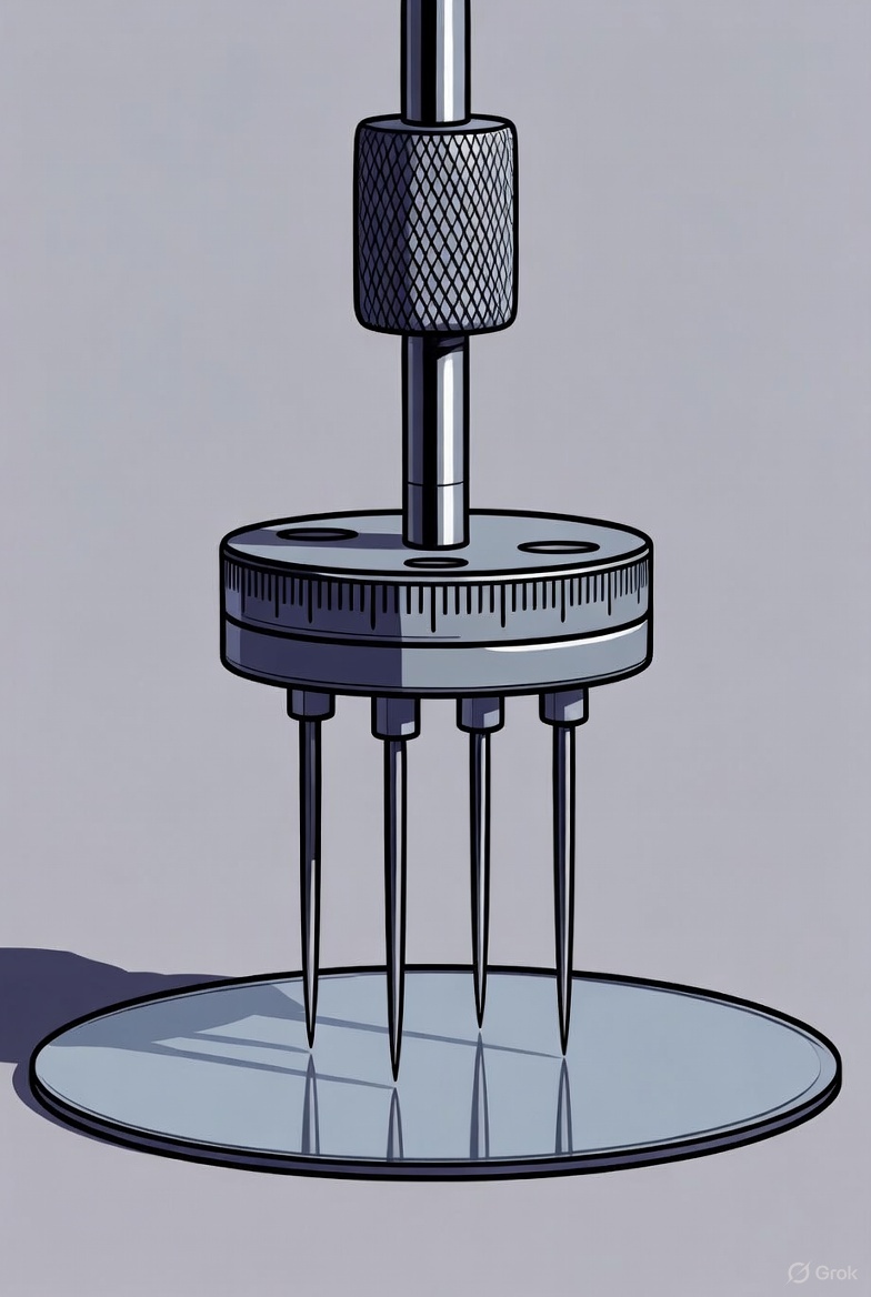
The Four-Point Probe (4PP) method is a standard, non-destructive technique used in semiconductor manufacturing and research to accurately measure the sheet resistance and subsequent resistivity of thin films, wafers, and other semiconductor materials. This technique uses a linear array of four closely spaced, collinear probes typically made of tungsten or beryllium copper, each mounted on…
-
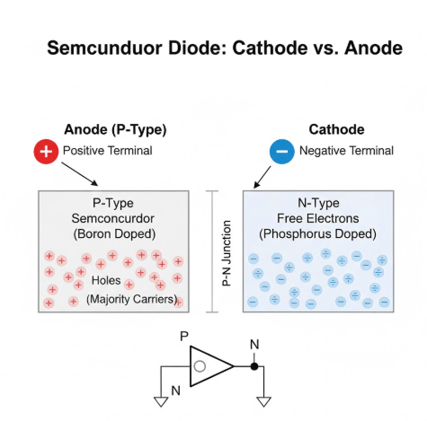
The cathode is the terminal of an electrical device through which current flows out of the device in conventional current terms (positive to negative). In a diode, the cathode is typically marked with a stripe and is the side connected to the negative voltage during forward bias. It is the terminal where electrons enter the…
-
A diode is a two-terminal semiconductor device that permits current to flow primarily in one direction, making it a fundamental component in electronics. Electrical characterization of diodes involves analyzing their current–voltage (I–V) relationship, which reveals distinct operating regions. In a diode, the anode and cathode are the two terminals that define its directionality and electrical…
-

In semiconductor technology, particularly within the foundational Metal-Oxide-Semiconductor (MOS) structure, oxide charges represent a critical class of parasitic defects—localized electric charges trapped either within the gate oxide layer (typically silicon dioxide) or at its delicate interface with the semiconductor substrate. These charges are not intentional but are inevitable byproducts of fabrication imperfections, chemical contamination, or…
-
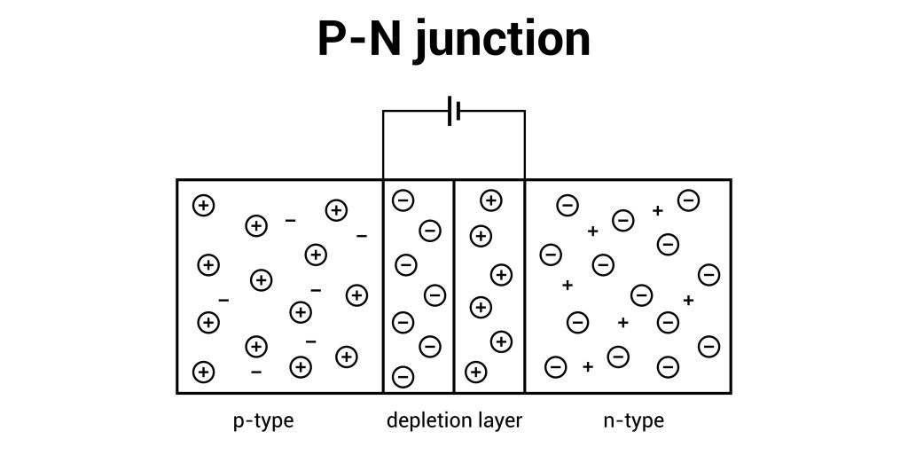
A p-n junction diode is the simplest form of a semiconductor electronic device, created by joining a p-type and an n-type semiconductor material within a single crystal. The p-type material is doped with acceptor impurities, resulting in an excess of holes (positive charge carriers), while the n-type material is doped with donor impurities, resulting in…
-

The I-V characteristics of a diode describe how the electric current flowing through the device responds to changes in the voltage applied across its terminals. In forward bias, when the positive terminal of a voltage source is connected to the diode’s anode and the negative to its cathode, the diode initially resists current flow until…
-

The band gap is the energy difference between the top of the valence band and the bottom of the conduction band in a solid. It represents the minimum energy required to excite an electron from a bound state in the valence band to a free state in the conduction band. The size of the band…
-
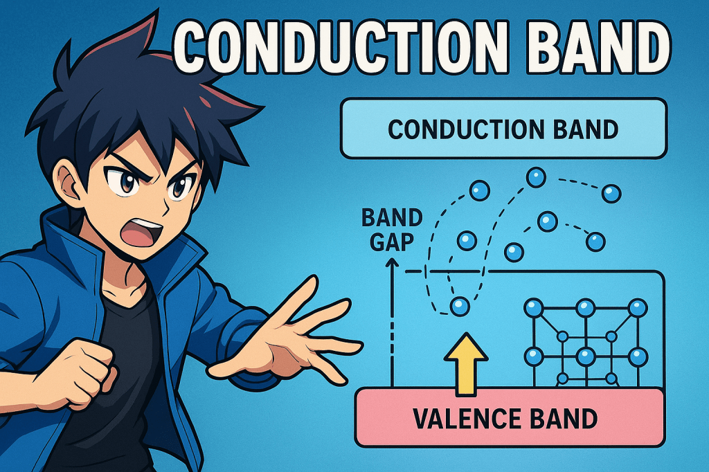
The conduction band is the range of electron energies in a solid where electrons are free to move and contribute to electrical conduction. It lies above the valence band and is typically empty at absolute zero temperature. When electrons gain sufficient energy to jump from the valence band to the conduction band, they become delocalized…
-
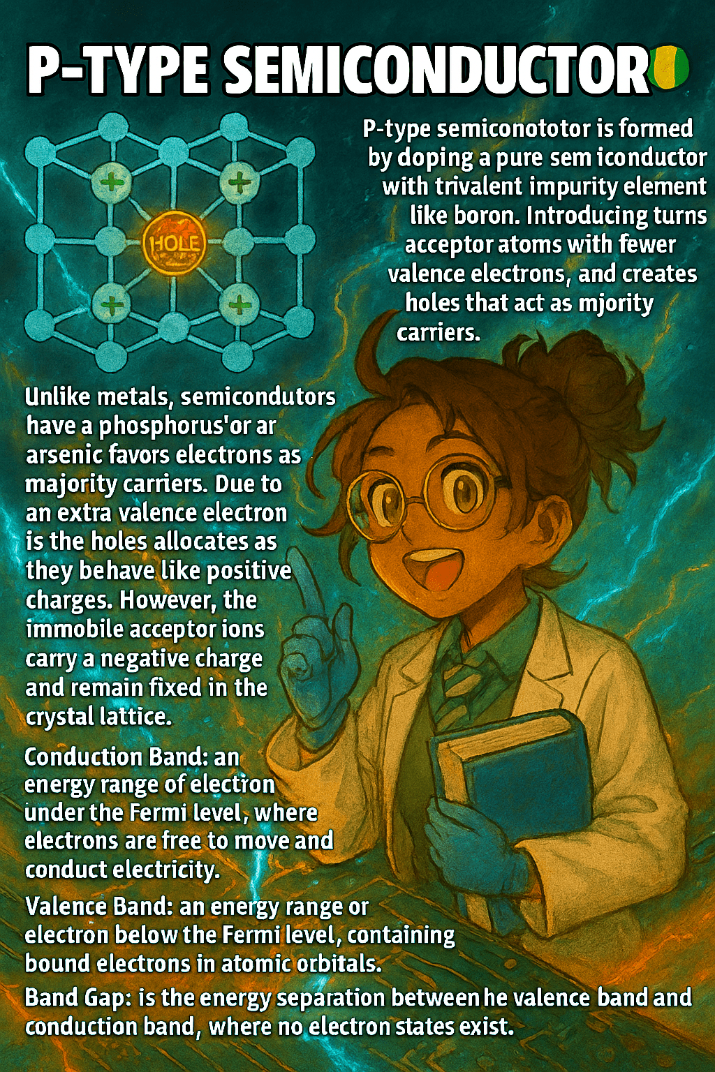
A p-type semiconductor is formed by doping a pure semiconductor, such as silicon, with trivalent elements like boron, gallium, or indium. These dopants have only three valence electrons, one fewer than silicon, which creates a vacancy or “hole” in the crystal lattice. Holes act as positive charge carriers because electrons from neighboring atoms can move…
-

The valence band is the highest range of electron energies in a solid where electrons are normally present at absolute zero temperature. These electrons are bound to atoms and participate in chemical bonding, such as covalent or metallic bonds. In crystalline solids, the valence band is formed by the overlap of atomic orbitals, creating a…
-
An n-type semiconductor is created by doping a pure semiconductor, such as silicon, with pentavalent elements like phosphorus, arsenic, or antimony. These dopants have five valence electrons, one more than silicon, and the extra electron becomes loosely bound and available for conduction. As a result, electrons become the majority charge carriers in n-type materials, while…
-

Silicon is a chemical element with atomic number 14, belonging to Group 14 of the periodic table, and it is the most widely used semiconductor material. Its electron configuration is [Ne] 3s² 3p², meaning it has four valence electrons available for bonding. In its crystalline form, silicon adopts a diamond cubic lattice structure, where each…
-

Semiconductors are materials whose electrical conductivity lies between that of conductors and insulators, and they are unique because their properties can be controlled and modified. Semiconductors are chemically diverse materials whose electrical conductivity lies between that of conductors and insulators, and their behavior can be precisely engineered. The most common elemental semiconductors are silicon (Si),…
-

Insulators are materials that resist the flow of electric current because their electrons are tightly bound to their atoms and cannot move freely. This high resistivity makes them ideal for preventing unwanted current flow and protecting users from electrical hazards. Common examples include rubber, glass, porcelain, and plastic, all of which are widely used to…
-

Resistivity is a fundamental property of materials that describes how strongly they oppose the flow of electric current. Unlike resistance, which depends on the dimensions of a conductor, resistivity is an intrinsic characteristic that remains constant for a given material under specific conditions. It is mathematically expressed as, where is the resistance, is the cross-sectional…
-

In semiconductor crystals, the atomic arrangement is defined by a combination of a Bravais lattice and a basis. The Bravais lattice provides the geometric framework—an infinite array of points arranged with translational symmetry—where each point has an identical environment. There are 14 unique Bravais lattices in three dimensions, grouped into seven crystal systems such as…
-

Transmission electron microscopy (TEM) is a powerful imaging technique that uses a beam of electrons transmitted through an ultrathin specimen to produce highly magnified images of its internal structure. TEM works by directing electrons through a sample that is typically less than 100 nanometers thick. As the electrons pass through, they interact with the atoms…
