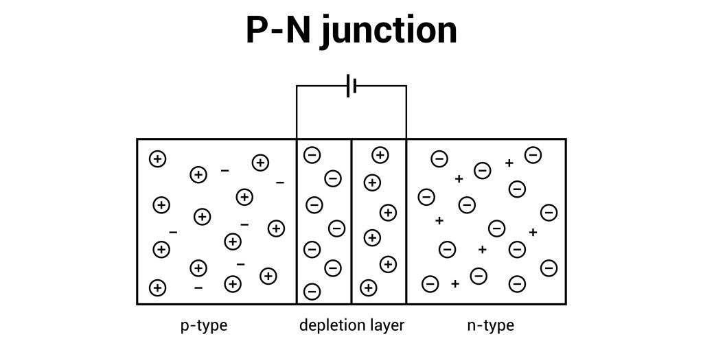
A p-n junction diode is the simplest form of a semiconductor electronic device, created by joining a p-type and an n-type semiconductor material within a single crystal.
The p-type material is doped with acceptor impurities, resulting in an excess of holes (positive charge carriers), while the n-type material is doped with donor impurities, resulting in an excess of free electrons (negative charge carriers).
At the moment of contact, the majority carriers near the interface diffuse across the boundary—electrons from the n-side move to the p-side, and holes from the p-side move to the n-side—and recombine.
This recombination process leaves behind immobile, positively charged donor ions on the n-side and immobile, negatively charged acceptor ions on the p-side, forming a region devoid of mobile charge carriers called the depletion region or space-charge region.
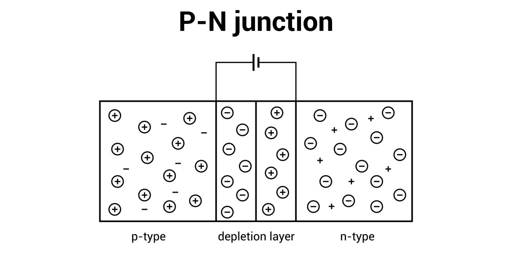
Image Credit: Shutterstock
This fixed charge creates an internal electric field that establishes a potential barrier across the junction, which prevents further majority carrier flow and gives the diode its essential functionality.
The p-n junction’s defining characteristic is its ability to allow electric current to flow effectively in only one direction (forward bias) while largely blocking it in the reverse direction (reverse bias), making it useful for applications like rectification, which converts alternating current (AC) to direct current (DC).
BitcoinVersus.Tech Editor’s Note:
We volunteer daily to ensure the credibility of the information on this platform is Verifiably True.
If you would like to support to help further secure the integrity of our research initiatives, please donate here: bc1qrved9tfquym6u3age7xhmnkjs2lq8j9aulperagkuhtuk5w5c35ssfpge8
BitcoinVersus.tech is not a financial advisor. This media platform reports on financial subjects purely for informational purposes.


Leave a comment