Elementary Overview
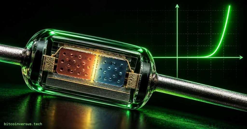
A diode is a tiny electronic part that makes it much easier for electric current to move in one direction than the other. Inside a common semiconductor diode are two regions of material called p-type and n-type semiconductor. Where those two regions meet, they form a PN junction. That junction behaves like a controllable gate for moving electric charge and charge carriers.
When forward voltage is applied, the gate becomes easier for charge carriers to cross, so current rises very quickly. When reverse voltage is applied, the gate becomes harder to cross and very little current normally flows. The rest of this lesson explains, with engineering equations, why that happens, how temperature changes the behavior, and how engineers describe a real diode using resistance and capacitance as well as current and voltage.
A PN-junction diode turns the electrostatics from OSSEC.003 into measurable current: forward bias lowers the carrier barrier, injects minority carriers into the quasi-neutral regions, and produces the exponential current–voltage behavior described by the Shockley equation. This lesson builds directly on OSSEC.003: PN Junction Electrostatics, OSSEC.002: Carrier Transport, and the earlier BitcoinVersus guide to current flow in a PN-junction diode.
Minority-Carrier Injection Creates Forward Current
Under forward bias, the external voltage reduces the junction barrier and raises the minority-carrier concentrations at the depletion-region edges. Those excess electrons and holes then diffuse through the quasi-neutral regions and recombine over characteristic diffusion lengths. This is why the drift, diffusion, mobility, and recombination concepts from OSSEC.002 are not optional background—they are the transport engine behind the diode’s forward current.
The Shockley Equation
For an idealized PN junction under low-level injection and the usual one-dimensional assumptions, terminal current is approximated by the Shockley diode equation. The exponential term means that once forward bias exceeds a few thermal voltages, relatively small changes in diode voltage can produce very large changes in current. The equation is a compact result of the carrier boundary conditions, continuity equation, diffusion transport, and recombination assumptions—not a standalone empirical rule.
- I = IS[exp(VD/(nVT)) − 1]
- I: diode current.
- IS: reverse saturation or scale current.
- VD: junction voltage.
- VT = kT/q: thermal voltage, about 25.9 mV at 300 K.
- n: ideality factor.
Reverse Saturation Current Is a Device Parameter
The scale current IS is set by semiconductor material, junction area, doping, minority-carrier diffusion coefficients, diffusion lengths, lifetime, and temperature. In the ideal long-base model it is proportional to terms such as qADnnp0/Ln and qADppn0/Lp. Because equilibrium minority-carrier concentrations depend strongly on intrinsic carrier concentration, IS is extremely temperature-sensitive and can change by orders of magnitude across a practical operating range.
Ideality Factor Explains Non-Ideal Current Slopes
The ideality factor n modifies the exponential slope of the I–V curve and helps identify which transport or recombination mechanism dominates. A diffusion-dominated ideal PN junction is close to n = 1; depletion-region Shockley–Read–Hall recombination can push behavior toward n ≈ 2. Real measured values can shift with current density because series resistance, high-level injection, tunneling, interface defects, and other mechanisms violate the assumptions of the simplest model.
Temperature Changes Both Thermal Voltage and Saturation Current
Temperature enters the diode equation directly through VT = kT/q and indirectly through the much stronger temperature dependence of IS. At a fixed forward current, a conventional silicon diode therefore tends to require less forward voltage as temperature rises. That behavior makes a diode useful as a temperature sensor but also creates thermal-design concerns in power electronics, where current crowding and self-heating can reinforce one another unless the circuit and package provide adequate stabilization and heat removal.
Forward Bias Stores Minority-Carrier Charge
A forward-biased diode stores excess minority carriers in its quasi-neutral regions. When terminal voltage changes, that stored charge changes, producing diffusion capacitance. Unlike depletion capacitance, which is especially important under reverse bias and was introduced in OSSEC.003, diffusion capacitance becomes important when substantial forward current exists and helps explain diode switching delay and reverse-recovery behavior.
Dynamic Resistance Linearizes the Exponential Curve Locally
For a small AC signal riding on a DC operating point, the nonlinear diode can be linearized by taking the local slope of its I–V characteristic. The resulting dynamic or diffusion resistance is approximately rd = nVT/ID when the forward current is much larger than IS. This is a differential quantity, not the same thing as the large-signal ratio V/I, and it changes whenever bias current or temperature changes.
The Complete Small-Signal Model Combines Resistance and Capacitance
A practical small-signal diode model can include dynamic resistance, depletion capacitance, diffusion capacitance, and parasitic series or contact resistance. That model is the bridge from semiconductor physics to circuit analysis in rectifiers, detectors, mixers, clamps, sensors, switching networks, and RF systems. Technicians can verify real devices with a correctly configured digital multimeter, while engineers can compare bench data against KiCad or SPICE-based circuit models and the device manufacturer’s datasheet.
Worked Engineering Example
- Assume a silicon diode at 300 K with n = 1.5, IS = 1 nA, and VD = 0.60 V.
- Use VT ≈ 25.9 mV.
- The exponent is VD/(nVT) ≈ 15.44.
- The idealized diode current is therefore approximately 5.1 mA.
- The small-signal resistance at that operating point is approximately rd = nVT/I ≈ 7.6 Ω.
- If temperature changes, recalculate both VT and the strongly temperature-dependent IS; do not assume only one term changes.
Engineering Limits of the Shockley Model
- Very low current: generation-recombination and leakage can dominate.
- Moderate forward current: the Shockley relation is often most useful.
- High current: series resistance, conductivity modulation, and high-level injection can dominate.
- Strong reverse bias: breakdown physics replaces the simple reverse-saturation picture.
- Fast switching: stored charge and capacitances must be included.
- Small geometry / advanced materials: tunneling, interface states, quantum effects, self-heating, and field crowding can require more advanced models.
Exercises
- Starting from the Shockley equation, calculate current for IS = 10 pA, n = 1, T = 300 K, and VD = 0.65 V.
- Repeat the calculation for n = 2 and explain why the current changes.
- Plot ln(I) versus V for an ideal diode and show how the slope can be used to estimate ideality factor.
- Explain why increasing junction area tends to increase IS.
- Calculate rd at 100 µA, 1 mA, and 10 mA for n = 1 at 300 K.
- Describe the physical origin of diffusion capacitance.
- Explain why a fixed “0.7 V diode drop” is only an approximation, not a physical law.
- Use a digital multimeter diode-test function on a known good silicon diode and compare the measured forward voltage with the exponential model’s qualitative prediction.
- Build a SPICE diode model in KiCad or another simulator, sweep diode voltage, and compare the simulated I–V curve against the Shockley equation.
- List three mechanisms that can make an extracted ideality factor vary with current.
Knowledge Check + Answers
- What causes the exponential rise in forward current? Forward bias changes the minority-carrier boundary concentrations exponentially, producing exponentially increasing diffusion current under the ideal assumptions.
- What is thermal voltage? VT = kT/q; it is about 25.9 mV at 300 K.
- What does IS represent? The reverse saturation or scale current set by material, geometry, doping, carrier transport, lifetime, and temperature.
- What does ideality factor measure? It adjusts the exponential slope to represent departures from the ideal diffusion-current model and can reveal dominant recombination or transport mechanisms.
- Why is the diode’s forward voltage temperature-dependent? Both thermal voltage and especially saturation current change with temperature.
- What is diffusion capacitance? The incremental charge-storage effect caused by forward-injected minority carriers in the quasi-neutral regions.
- What is dynamic resistance? The inverse local slope of the diode I–V curve, approximately nVT/ID at useful forward bias.
- Why does the Shockley equation fail at high current? Series resistance, high-level injection, self-heating, and other non-ideal effects can dominate.
Key Takeaway
- Forward bias injects minority carriers.
- Minority-carrier diffusion and recombination produce the ideal exponential current relation.
- IS, n, and VT control the shape and scale of the I–V curve.
- Temperature strongly affects diode current.
- Stored charge creates diffusion capacitance.
- The local I–V slope creates dynamic resistance.
- Real circuit models combine semiconductor physics with resistance, capacitance, parasitics, and temperature.
Elementary Conclusion
In simple terms, a diode works because the inside of the device creates a tiny electrical boundary that charge carriers must cross. P-type and n-type semiconductor meet at the PN junction, and that junction changes depending on which way voltage is applied. Forward voltage makes the barrier easier to cross, so current can grow quickly. Reverse voltage makes the barrier harder to cross, so the diode mostly blocks current unless the reverse voltage becomes large enough to cause breakdown.
The equations in this lesson are detailed ways of describing that simple idea. The Shockley equation tells engineers how fast current rises, the ideality factor helps describe how closely a real diode follows the simplest theory, temperature changes how easily charge moves, and the diode’s resistance and capacitance describe how it behaves when signals change over time. A useful mental picture is therefore not just “a one-way switch,” but a tiny semiconductor gate whose behavior depends on voltage, temperature, stored charge, and the physical structure of the material.
BitcoinVersus.Tech
Advertisement
Editor’s Note:
We volunteer daily to ensure the credibility of the information on this platform is Verifiably True. If you would like to support our research initiatives, please donate here: 3C9o19EH5HSiwEPyCTmEKzxhNCbo2X6TTb
BitcoinVersus.tech is not a financial advisor. This media platform reports on financial subjects purely for informational purposes.


Leave a Reply