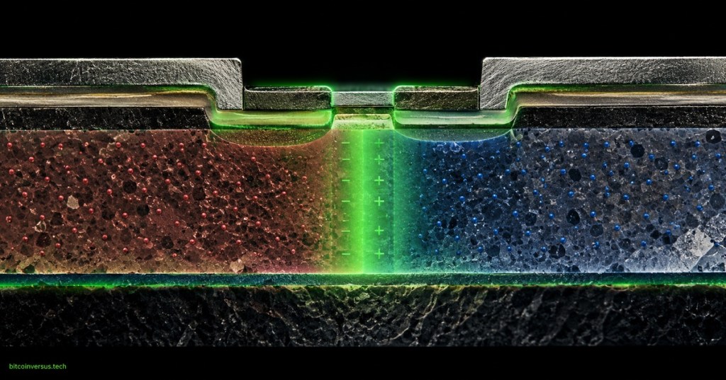
A PN junction is an electrostatic structure before it is a diode equation: diffusion leaves behind fixed ionized dopants, those charges create a depletion region and electric field, and that field establishes the built-in potential that controls junction behavior.
OSSEC.003 continues the semiconductor-engineering sequence from OSSEC.001: Semiconductor Device Physics — Band Gaps, Doping, and PN Junctions and OSSEC.002: Carrier Transport — Drift, Diffusion, Mobility, and Recombination. It also connects device physics to the process environment covered in OSSTC.003: Semiconductor Vacuum Systems.
The abrupt PN junction as an electrostatic boundary-value problem
When p-type and n-type semiconductor regions are joined, majority carriers initially diffuse across the metallurgical junction. Electrons leave the n side and holes leave the p side. Near the junction, that diffusion uncovers fixed ionized donors on the n side and fixed ionized acceptors on the p side. The resulting space charge creates an electric field that opposes further majority-carrier diffusion.
At thermal equilibrium, the drift and diffusion tendencies balance. There is no net terminal current, but the junction contains a nonzero electric field and a built-in electrostatic potential.
Depletion approximation
The introductory abrupt-junction model uses the depletion approximation. Mobile carriers are treated as strongly depleted from a region extending a distance xp into the p side and xn into the n side. Outside that region, the semiconductor is treated as approximately charge neutral.
- On the depleted p side, the dominant fixed charge density is approximately −qNA.
- On the depleted n side, the dominant fixed charge density is approximately +qND.
- The total depletion width is W = xp + xn.
- The depletion approximation is most useful when an abrupt doping transition and classical electrostatics are reasonable first-order models.
Lecture: PN junction formation and equilibrium
Charge neutrality determines how depletion width divides
The net uncovered positive and negative charge must balance for the ideal one-dimensional abrupt junction:
NAxp = NDxn
This relation immediately shows that the depletion region extends farther into the more lightly doped side. Solving together with W = xp + xn gives:
xp = W · ND/(NA + ND)
xn = W · NA/(NA + ND)
If NA ≫ ND, most of the depletion region lies in the n material. The opposite is true when the n side is much more heavily doped.
Built-in potential
For a nondegenerate abrupt silicon PN junction under the usual equilibrium assumptions, the built-in potential is approximated by:
Vbi = VT ln[(NAND)/ni2]
- VT = kT/q, the thermal voltage.
- NA and ND are acceptor and donor concentrations.
- ni is the intrinsic carrier concentration for the material and temperature.
At approximately 300 K, VT ≈ 25.9 mV. The logarithm means built-in potential changes more slowly than doping concentration itself, but it still shifts with doping and temperature.
Poisson’s equation links charge to field and potential
Electrostatics inside the junction follows Poisson’s equation:
dE/dx = ρ/εs
Because the depletion approximation treats the space-charge density as approximately constant on each side of an abrupt junction, the electric field changes linearly with position inside the depleted region. The field is zero at the ideal depletion edges and reaches its largest magnitude at the metallurgical junction.
The peak electric-field magnitude can be written as:
|Emax| = qNDxn/εs = qNAxp/εs
For the ideal abrupt junction, the field profile is triangular. The potential drop across the depletion region is the area under that field profile:
Vj = ½|Emax|W
Depletion width equation
Combining charge neutrality, Poisson’s equation, and the potential drop gives the standard abrupt-junction depletion width:
W = √[(2εs/q)(1/NA + 1/ND)(Vbi − VA)]
Here VA is defined positive for forward bias. Under reverse bias, VA is negative, so Vbi − VA increases and the depletion region widens.
Worked lecture: depletion width and electric field
Forward bias lowers the electrostatic barrier
A positive p-side voltage relative to the n side is forward bias. In the sign convention above, forward bias reduces the depletion-region potential from approximately Vbi toward Vbi − VA. The depletion width decreases, and carrier injection across the junction becomes much easier.
The electrostatic model does not by itself produce the full diode current equation. The exponential current-voltage behavior additionally requires minority-carrier injection, diffusion, recombination assumptions, and boundary conditions. Those transport concepts were introduced in OSSEC.002.
Reverse bias raises the barrier and widens depletion
Reverse bias increases the total junction potential and widens the depletion region. The stronger field and wider depleted volume are central to photodiodes, avalanche devices, high-voltage rectifiers, power MOSFET body diodes, and many sensor structures.
Reverse bias cannot be increased indefinitely. At sufficiently large field, breakdown mechanisms such as Zener tunneling or avalanche multiplication can dominate. The detailed breakdown regime depends on doping, junction geometry, material, temperature, and field profile.
Junction capacitance is electrostatics expressed as charge storage
The depletion region separates fixed positive and negative charge. A change in applied voltage changes depletion width and therefore changes stored charge. This creates a voltage-dependent junction capacitance.
For an abrupt planar junction, the depletion capacitance is approximately:
Cj = εsA/W
As reverse bias increases, W increases and Cj decreases. This is the operating principle behind varactor diodes and a key reason C–V measurements can reveal doping information.
Lecture: PN junction capacitance
One-sided abrupt junction approximation
When one side is much more heavily doped than the other, the junction is often treated as one-sided. For example, in a p+n structure with NA ≫ ND, nearly all depletion width lies in the lightly doped n side. The width then simplifies approximately to:
W ≈ √[2εs(Vbi + VR)/(qND)]
This approximation is central to high-voltage device engineering because the lightly doped drift region is intentionally designed to support much of the reverse-bias potential.
Numerical engineering example
Consider an abrupt silicon junction at approximately 300 K with NA = 1×1017 cm−3, ND = 1×1016 cm−3, and ni ≈ 1×1010 cm−3.
- The built-in potential is approximately 0.774 V.
- Using silicon permittivity, the zero-bias depletion width is approximately 0.332 µm.
- Charge neutrality places only about 0.030 µm of that width in the more heavily doped p side and about 0.302 µm in the n side.
- The peak electric field is approximately 46.6 kV/cm in this idealized model.
- For a 100 µm × 100 µm junction area, the zero-bias depletion capacitance is approximately 3.12 pF.
- At 5 V reverse bias, the depletion width rises to approximately 0.906 µm, reducing the same idealized junction capacitance to approximately 1.14 pF.
This example shows the coupled design tradeoff: lighter doping and greater reverse bias increase depletion width and reduce capacitance, but they also change electric-field distribution and breakdown behavior.
C–V measurement as a process and device-engineering tool
Capacitance-versus-voltage measurement converts an electrostatic model into measurable process information. For an ideal one-sided abrupt junction, a plot of 1/C2 versus applied voltage is approximately linear. Its slope can be related to doping concentration, and its voltage-axis intercept can be related to built-in potential under the model assumptions.
- Unexpected capacitance can indicate geometry variation, doping variation, parasitics, interface effects, or measurement setup problems.
- A nonideal C–V slope can reveal a graded profile instead of an abrupt profile.
- Frequency dependence can expose traps, interface states, series resistance, or minority-carrier response.
- Guard structures and test-fixture parasitics matter when the junction capacitance is very small.
Process variation changes electrostatics
Junction electrostatics depend on the actual activated dopant profiles and geometry, not only the implant recipe. Semiconductor process steps can shift depletion width, built-in potential, leakage, capacitance, and breakdown behavior.
- Implant dose: changes intended dopant concentration.
- Implant energy: changes depth distribution.
- Anneal conditions: affect activation, diffusion, and damage recovery.
- Thermal budget: changes junction depth and gradient.
- Crystal defects: can add leakage and field-localization paths.
- Surface and isolation geometry: alter two-dimensional field crowding relative to the one-dimensional textbook model.
- Metrology error: can make a good device look electrically inconsistent if area, temperature, probe parasitics, or calibration are wrong.
Field crowding and why real junctions are not one-dimensional
The planar abrupt-junction equations are foundational, but real devices contain corners, curved junctions, trench structures, guard rings, field plates, isolation boundaries, contacts, and nonuniform doping. Electric field can crowd at curvature or geometry transitions, producing local peak fields larger than a simple one-dimensional estimate.
This is why high-voltage junction design uses termination structures. A device can have an acceptable bulk doping level yet fail prematurely if edge termination allows local field concentration.
Connection to device simulation
Classical semiconductor device simulation couples Poisson’s equation to carrier continuity and drift-diffusion equations. OSSEC.002 introduced the transport side; this lesson supplies the electrostatic structure. Together they define the minimum classical framework for numerical PN-junction, diode, BJT, MOS capacitor, and transistor analysis.
MIT OpenCourseWare’s Microelectronic Devices and Circuits lecture notes provide a useful university reference for the progression from semiconductor statistics through PN-junction electrostatics and device behavior.
Engineering troubleshooting framework
When measured junction capacitance, leakage, or breakdown does not match expectation, a disciplined investigation should separate electrostatic, process, geometry, and measurement causes.
- Confirm device area, test structure identity, temperature, and probe configuration.
- Verify the intended p-side and n-side doping levels and activation.
- Compare measured C–V against the abrupt or graded-junction model that actually matches the process.
- Check whether series resistance or measurement frequency distorts capacitance.
- Look for edge leakage, guard-ring problems, junction curvature, or field crowding.
- Compare leakage and breakdown distributions across wafer position.
- Correlate electrical behavior with implant, anneal, diffusion, oxide, and contamination metrology.
- Use device simulation only after the physical structure and measurement assumptions are internally consistent.
Exercises
- Derive the charge-neutrality relation NAxp = NDxn from equal and opposite uncovered depletion charge.
- For a junction with NA = 10ND, determine what fraction of total depletion width lies on each side.
- Calculate built-in potential for supplied values of NA, ND, ni, and temperature.
- Explain why the electric-field profile is linear inside each side of the depletion region under the abrupt-junction approximation.
- Calculate zero-bias depletion width for a specified silicon junction.
- Repeat the width calculation under 3 V reverse bias and explain the direction of the change.
- Calculate depletion capacitance for a specified device area.
- Explain why the more lightly doped side supports more of the depletion width.
- List three process changes that could move a measured C–V curve away from design intent.
- Explain why edge termination matters even when the one-dimensional bulk-junction calculation predicts adequate breakdown margin.
Knowledge check
1. What creates the depletion-region electric field?
Fixed ionized donors and acceptors exposed after mobile majority carriers diffuse away from the junction region.
2. Why does the depletion region extend farther into the lightly doped side?
More physical width is required on the lightly doped side to uncover enough fixed charge to balance the charge on the heavily doped side.
3. What is the built-in potential?
The equilibrium electrostatic potential difference established across the junction by carrier diffusion and the resulting space-charge field.
4. What does forward bias do to depletion width?
It reduces the junction potential barrier and narrows the depletion region.
5. What does reverse bias do to depletion width?
It increases the junction potential and widens the depletion region.
6. Why does junction capacitance decrease under reverse bias?
The depletion width increases, and Cj = εsA/W.
7. What equation connects charge density to electric-field gradient?
Poisson’s equation, written in one dimension as dE/dx = ρ/εs.
8. Why can a real device break down earlier than a one-dimensional calculation predicts?
Two-dimensional field crowding at curvature, edges, contacts, or imperfect termination can create a larger local peak field.
Key takeaway
A PN junction is governed by coupled charge, field, and potential. Doping determines how depletion charge is distributed; Poisson’s equation determines the electric field; the field integrates to the junction potential; applied bias changes depletion width; and that changing width produces voltage-dependent junction capacitance. These relationships form the electrostatic foundation for diode current, C–V metrology, breakdown engineering, power-device design, photodiodes, and transistor junctions.
Modeling note: the equations above use an introductory abrupt-junction depletion approximation. Degenerate doping, graded profiles, high injection, tunneling, quantum confinement, strong interface effects, and nanoscale geometries can require more advanced models.
Display note: this lesson uses standard Gutenberg paragraphs, headings, lists, and media embeds without decorative text-box layouts, reducing the risk of clipped or overflowing text on narrow screens.
BitcoinVersus.Tech
Advertisement
Editor’s Note:
We volunteer daily to ensure the credibility of the information on this platform is Verifiably True. If you would like to support our research initiatives, please donate here: 3C9o19EH5HSiwEPyCTmEKzxhNCbo2X6TTb
BitcoinVersus.tech is not a financial advisor. This media platform reports on financial subjects purely for informational purposes.


Leave a Reply