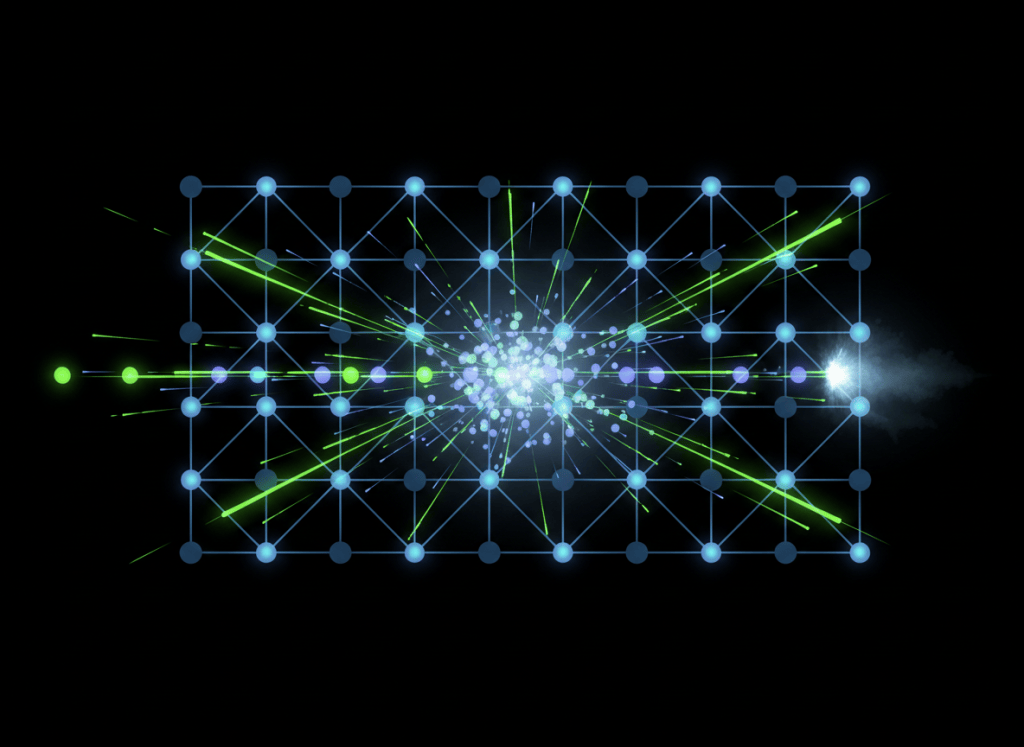
Semiconductor device behavior depends not only on how many carriers exist, but on how electrons and holes move, scatter, diffuse, recombine, and respond to electric fields.
OSSEC.002 continues the semiconductor-engineering sequence established in OSSEC.001: Semiconductor Device Physics — Band Gaps, Doping, and PN Junctions. It also connects device-level transport theory to the manufacturing environment introduced in OSSTC.002: Wafer Handling, FOUPs, and Automated Material Flow Basics.
Carrier transport is the bridge between electrostatics and current
Band structure and doping establish the available states and equilibrium carrier concentrations. Current appears when carriers acquire a net directed motion or when spatial concentration gradients cause a net flux.
- Drift: carrier motion driven by an electric field.
- Diffusion: carrier motion driven by a concentration gradient.
- Mobility: proportionality between low-field drift velocity and electric field.
- Scattering: microscopic interactions that limit carrier momentum and mobility.
- Generation: creation of electron-hole pairs or carriers through thermal, optical, or other mechanisms.
- Recombination: removal of an electron and hole from the mobile carrier populations.
These mechanisms appear in resistors, PN junctions, MOSFETs, photodiodes, solar cells, LEDs, image sensors, power devices, and nearly every semiconductor structure that carries charge.
1. Thermal motion does not automatically create net current
Electrons and holes in a semiconductor undergo rapid microscopic motion even at thermal equilibrium. The directions are random, so the average directed velocity is zero when no net driving force or gradient exists.
Current requires an imbalance in that random motion. An electric field creates one type of imbalance; a concentration gradient creates another.
2. Drift velocity and mobility
In the low-field regime, the average drift velocity is approximately proportional to electric field:
vdn = −μnE
vdp = +μpE
- vdn, vdp = electron and hole drift velocities
- μn, μp = electron and hole mobilities
- E = electric field
The negative sign for electrons reflects their negative charge. Conventional current still points in the direction defined for positive charge flow.
Video 1: Drift current and mobility
3. Drift current density
The conventional drift-current densities are:
Jn,drift = q n μnE
Jp,drift = q p μpE
Total drift current density is therefore:
Jdrift = q(n μn + p μp)E
This expression connects directly to semiconductor conductivity:
σ = q(n μn + p μp)
The relationship shows why carrier concentration and mobility are separate engineering variables. A process can increase carrier concentration while simultaneously reducing mobility through increased impurity scattering.
4. Mobility is not a universal constant
Mobility depends on semiconductor material, temperature, doping, electric field, crystal quality, strain, interface quality, and other scattering mechanisms.
- Lattice scattering: carrier interactions with crystal vibrations.
- Ionized impurity scattering: carrier deflection by charged dopant ions.
- Surface or interface scattering: important near oxide-semiconductor interfaces and confined channels.
- Defect scattering: caused by imperfections, dislocations, damage, or other structural disturbances.
At ordinary low electric fields, mobility-based linear transport is useful. At high fields, carrier velocity becomes nonlinear and may approach a saturation regime, so the simple proportional relationship is no longer sufficient.
5. Diffusion begins with a concentration gradient
Diffusion occurs when carrier concentration changes with position. Random carrier motion causes more particles to leave a high-concentration region than enter it from a low-concentration region, producing a net flux.
The one-dimensional particle-flux form of Fick’s law is proportional to the negative concentration gradient. Semiconductor current equations must also account for the carrier charge sign.
For electrons and holes in one dimension:
Jn,diff = qDn(dn/dx)
Jp,diff = −qDp(dp/dx)
- Dn, Dp = electron and hole diffusion coefficients
- dn/dx, dp/dx = spatial carrier-concentration gradients
The opposite signs result from the opposite charges carried by electrons and holes.
Video 2: Diffusion current and the Einstein relation
6. Drift and diffusion usually operate together
The general one-dimensional electron and hole current densities combine both mechanisms:
Jn = qnμnE + qDn(dn/dx)
Jp = qpμpE − qDp(dp/dx)
In many devices, the electric field and concentration gradient are both consequences of the same underlying electrostatics. Separating drift and diffusion is mathematically useful, but the physical device experiences both simultaneously.
7. Equilibrium can contain opposing transport mechanisms
A PN junction in thermal equilibrium illustrates the balance clearly. Carrier gradients drive diffusion away from the high-concentration side, while the built-in electric field drives drift in the opposite direction.
At equilibrium:
drift current + diffusion current = 0
This does not mean carriers stop moving. It means the opposing net current components cancel.
8. The Einstein relation links diffusion and mobility
For a nondegenerate semiconductor in thermal equilibrium, mobility and diffusion coefficient are related by:
D / μ = kT / q
At approximately 300 K, kT/q ≈ 25.9 mV.
The Einstein relation is important because it shows that drift and diffusion are not unrelated empirical effects. Both arise from the same carrier statistics and scattering physics under the assumptions of the model.
MIT OpenCourseWare’s Microelectronic Devices and Circuits sequence places carrier transport immediately after semiconductor statistics and before PN-junction device analysis, reflecting the central role of drift and diffusion in device physics.
9. Scattering determines how momentum is lost
An electric field accelerates carriers between scattering events. Scattering randomizes part of the directed momentum and limits the average drift velocity.
A simplified mobility picture can be expressed through a mean momentum-relaxation time:
μ ≈ qτm / m*
- τm = effective momentum-relaxation time
- m* = carrier effective mass
This simple expression makes two engineering ideas visible: longer momentum retention supports greater mobility, while larger effective mass reduces acceleration for the same applied force.
10. High-field transport changes the model
At sufficiently high electric field, drift velocity no longer increases linearly with field. Energy gained from the field changes the carrier distribution and scattering rates. Silicon transport can enter a velocity-saturation regime, and short devices can require nonlocal or quasi-ballistic models.
This transition is one reason modern transistor design cannot rely only on low-field mobility. Channel length, electric-field profile, strain, interface quality, contact resistance, and carrier injection all interact.
11. Generation and recombination change carrier population
Transport equations describe movement, but device behavior also depends on whether carriers are being created or removed.
- Generation: an electron transitions into a mobile state while a corresponding hole or other carrier-state change is produced.
- Recombination: an electron returns to an available lower-energy state, removing an electron-hole pair from the mobile populations.
Generation-recombination behavior controls minority-carrier lifetime, leakage, transient response, photodetection, LED emission, solar-cell collection, and many PN-junction effects.
Video 3: Generation and recombination
12. Major recombination mechanisms
- Band-to-band radiative recombination: electron-hole recombination releases energy as a photon; especially important in direct-band-gap optoelectronic materials.
- Shockley-Read-Hall recombination: defect or trap states inside the band gap mediate recombination.
- Auger recombination: recombination energy is transferred to another carrier rather than directly emitted as a photon.
- Surface recombination: interface states provide efficient recombination paths at exposed or imperfect surfaces.
The dominant mechanism depends on material, injection level, defect density, interface quality, doping, temperature, and device structure.
13. Carrier lifetime
Carrier lifetime is a characteristic time scale describing how quickly an excess carrier population returns toward equilibrium under a specified recombination model.
A simple low-level excess-carrier decay can be written conceptually as:
Δn(t) = Δn(0)e−t/τ
Here τ is an effective lifetime under the assumed conditions. Real devices can require multiple recombination channels and position-dependent lifetimes.
14. Diffusion length combines lifetime and transport
A minority carrier does not diffuse indefinitely before recombination. A useful characteristic diffusion length is:
L = √(Dτ)
This relationship connects transport quality and recombination quality. Greater diffusion coefficient or longer lifetime increases the characteristic distance an excess carrier can travel before recombining.
15. Continuity equations enforce carrier accounting
Device simulation must account for current flow, generation, recombination, and time-dependent storage. The carrier continuity equations provide that bookkeeping.
In conceptual form:
rate of carrier change = transport in/out + generation − recombination
Combined with Poisson’s equation and current-density equations, continuity equations form the classical drift-diffusion device model used across semiconductor analysis and simulation.
16. Why process engineers care about mobility and lifetime
Mobility and lifetime are not abstract material constants detached from fabrication. Process steps can change them.
- Ion implantation can create lattice damage before annealing repairs and activates the dopants.
- Heavy doping increases ionized-impurity scattering.
- Interface defects can degrade surface mobility and increase recombination.
- Metal contamination can introduce deep levels that reduce lifetime.
- Crystal defects and dislocations can act as recombination centers.
- Thermal processing can change defect populations and dopant distributions.
- Strain engineering can alter band structure and carrier transport.
17. Engineering example: resistor sheet resistance
A doped semiconductor resistor illustrates the concentration-mobility tradeoff.
Increasing donor concentration usually increases electron concentration and tends to reduce resistivity. At the same time, stronger ionized-impurity scattering can reduce electron mobility. The final resistivity therefore depends on both variables rather than doping alone.
This is why sheet-resistance measurements are valuable process monitors: they respond to the combined electrical result of dose, activation, mobility, and geometry.
18. Engineering example: PN-junction minority carriers
Under forward bias, a PN junction injects minority carriers across the depletion region. Those carriers diffuse into the neutral regions and recombine over characteristic lengths controlled by diffusion coefficient and lifetime.
This explains why diffusion current, minority-carrier lifetime, and diffusion length appear naturally in diode current, switching, solar-cell collection, photodiode response, and bipolar-transistor operation.
19. Engineer’s troubleshooting framework
Suppose measured device resistance is too high or minority-carrier response is too short-lived. A transport-centered investigation can ask:
- Did active carrier concentration match target?
- Did mobility degrade because of heavier-than-expected doping or process damage?
- Did interface quality change?
- Did metal contamination or trap density increase recombination?
- Did thermal processing alter defect density or dopant activation?
- Is the electric field high enough that low-field mobility assumptions fail?
- Did geometry or contact resistance dominate the electrical measurement?
- Do lifetime, sheet-resistance, Hall, C-V, and I-V measurements tell a consistent story?
Transport equations identify the variables. Process metrology and electrical characterization identify which variable moved.
Exercises
- Derive the units of mobility from
vd = μE. - Calculate electron drift velocity for a stated electric field using a supplied low-field mobility.
- Write the electron and hole drift-current equations and explain the current-direction convention.
- Sketch a carrier-concentration profile and identify the direction of electron diffusion.
- Use the Einstein relation to estimate a diffusion coefficient from a supplied mobility at 300 K.
- Explain why drift and diffusion cancel in an equilibrium PN junction.
- Calculate a diffusion length from a supplied diffusion coefficient and lifetime.
- Identify one fabrication mechanism that can reduce mobility and one that can reduce carrier lifetime.
Knowledge check
1. What drives drift?
An electric field.
2. What drives diffusion?
A spatial carrier-concentration gradient.
3. What is mobility?
In the low-field model, mobility is the proportionality between average drift velocity and electric field.
4. Why can heavier doping reduce mobility?
Additional ionized dopants increase carrier scattering even while increasing carrier concentration.
5. What does the Einstein relation connect?
Diffusion coefficient and mobility through the thermal voltage kT/q under the model assumptions.
6. What is recombination?
A process that removes an electron and hole from the mobile carrier populations.
7. What does carrier lifetime represent?
A characteristic time scale for an excess carrier population to return toward equilibrium under specified recombination conditions.
8. What is diffusion length?
A characteristic distance an excess carrier can diffuse before recombination, commonly represented as L = √(Dτ).
Key takeaway
Semiconductor current is governed by both electrostatics and carrier transport. Electric fields produce drift, concentration gradients produce diffusion, scattering limits mobility, and generation-recombination processes control carrier population and lifetime. Together with Poisson’s equation and continuity equations, these ideas form the classical drift-diffusion framework used to analyze semiconductor devices.
Modeling note: equations in this lesson use introductory drift-diffusion assumptions. High-field, degenerate, ballistic, quantum-confined, strongly nonequilibrium, or nanoscale devices can require more advanced transport models.
Display note: this lesson uses standard Gutenberg paragraphs, headings, lists, code formatting, and media embeds only. No decorative text-box or callout-box layout is used.
BitcoinVersus.Tech
Advertisement
Editor’s Note:
We volunteer daily to ensure the credibility of the information on this platform is Verifiably True. If you would like to support our research initiatives, please donate here: 3C9o19EH5HSiwEPyCTmEKzxhNCbo2X6TTb
BitcoinVersus.tech is not a financial advisor. This media platform reports on financial subjects purely for informational purposes.


Leave a Reply