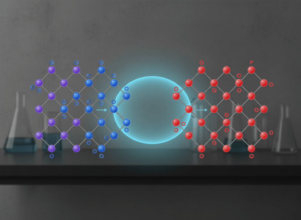
Semiconductor engineering starts with one idea: electrical behavior can be designed by controlling which energy states electrons can occupy and how many mobile charge carriers exist.
This is OSSEC.001, the first lesson in the Open Source Semiconductor Engineer Certification track. It builds on the technician-level cleanroom and ESD foundation from OSSTC.001 and moves into the physics engineers use to reason about devices and process tradeoffs.
The entire lesson in one model
atomic bonds
↓
allowed energy bands + forbidden band gap
↓
thermal energy creates electrons + holes
↓
doping changes carrier concentration and Fermi level
↓
P-type + N-type regions create a PN junction
↓
diffusion creates a depletion region + electric field
↓
bias changes the barrier
↓
current, capacitance, breakdown, speed, leakage, and device behavior
An engineer is not only asking, “Does the diode conduct?” The engineer asks why, how much, under what bias, at what temperature, and how the fabrication process changes the answer.
1. Why silicon is useful
In a crystal lattice, large numbers of atoms interact. Instead of treating every electron as occupying an isolated atomic energy level, solid-state physics describes groups of allowed energies called bands.
- Valence band: the highest band that is normally filled or nearly filled with bonding electrons.
- Conduction band: a higher-energy band in which electrons can move through the crystal and contribute strongly to conduction.
- Band gap, Eg: an energy range between those bands with no allowed bulk crystal states in the simplified model.
Energy ↑
Conduction band
↑
Eg ← band gap
↓
Valence band
Metals have available states that make conduction easy. Insulators have a comparatively large forbidden gap. Semiconductors occupy the useful middle ground: their conductivity can be changed dramatically by temperature, electric fields, light, and controlled impurity atoms.
MIT OpenCourseWare’s semiconductor lecture covers band gaps, charge carriers, intrinsic and extrinsic semiconductors, dopants, and conductivity as a unified picture. See MIT OpenCourseWare — Semiconductors.
Video 1: Semiconductor fundamentals
2. Electrons and holes are both charge carriers
When enough energy promotes a valence electron into the conduction band, two useful carrier descriptions appear:
- Electron: a mobile negative charge in the conduction band.
- Hole: an empty valence-band state that behaves mathematically like a mobile positive charge.
valence electron gains energy
↓
electron enters conduction band
↓
free electron + hole left behind
(−) and (+)
For an intrinsic semiconductor in equilibrium, electrons and holes are generated in pairs, so:
n = p = ni
Here n is electron concentration, p is hole concentration, and ni is the intrinsic carrier concentration. These values depend strongly on temperature and semiconductor material.
3. Conductivity depends on both concentration and mobility
A useful semiconductor conductivity relationship is:
σ = q(n μn + p μp)
- σ = conductivity
- q = magnitude of electron charge
- n, p = electron and hole concentrations
- μn, μp = electron and hole mobilities
This equation matters because increasing carrier concentration does not automatically improve every device property. Heavy doping can also change mobility, electric fields, junction capacitance, recombination, contact behavior, and breakdown characteristics.
4. Doping: intentionally changing the carrier population
Doping means intentionally introducing selected impurity atoms into a semiconductor so the equilibrium carrier population changes in a controlled way.
donor dopant
↓
adds an easily ionized electron state
↓
N-type material
↓
electrons become majority carriers
acceptor dopant
↓
creates an easily ionized hole state
↓
P-type material
↓
holes become majority carriers
In silicon, group-V elements such as phosphorus are commonly used as donors, while group-III elements such as boron are commonly used as acceptors. The exact choice depends on the material system and process integration.
A key engineering point: ordinary doping primarily changes carrier concentration and Fermi-level position. It does not simply “turn silicon into metal,” and it does not mean the crystal suddenly has a completely different ordinary band gap. At very heavy doping levels, additional effects such as band-gap narrowing and incomplete simple-model behavior become important.
Video 2: Intrinsic vs. extrinsic semiconductors
5. Majority and minority carriers
Doping does not remove the other carrier type.
N-type:
majority carrier → electrons
minority carrier → holes
P-type:
majority carrier → holes
minority carrier → electrons
Minority carriers matter enormously in diodes, bipolar transistors, photodiodes, solar cells, recombination, leakage, and transient behavior.
6. The mass-action relationship
For a nondegenerate semiconductor in thermal equilibrium, the electron and hole concentrations obey the mass-action relationship:
n · p = ni2
If donor doping pushes the electron concentration far above the intrinsic value, the equilibrium hole concentration becomes much smaller. The reverse is true for acceptor-doped P-type material.
For a simple room-temperature example, if a silicon region has an electron concentration around 1016 cm-3 and a model uses ni ≈ 1010 cm-3, then:
p = ni2 / n
= (1010)2 / 1016
= 104 cm−3
The purpose of this example is the orders-of-magnitude effect. Real ni values depend on temperature and the material/model used.
7. The Fermi level: the occupancy reference engineers track
The Fermi level is an energy reference connected to the probability that available states are occupied by electrons. In an equilibrium band diagram, it is one of the fastest ways to understand how carrier statistics and doping change carrier populations.
N-type doping → Fermi level shifts toward conduction band
P-type doping → Fermi level shifts toward valence band
This is why band diagrams are so useful: they let an engineer translate material composition and electrostatic potential into carrier behavior.
Stanford’s EE 116 semiconductor-device course sequence places energy bands, doping, Fermi level, drift, diffusion, PN diodes, MOS structures, and transistors in exactly this progression. See Stanford EE 116 — Semiconductor Device Physics.
8. Put P-type and N-type regions together: a PN junction
A PN junction is not normally manufactured by physically gluing separate chunks together. Engineers create neighboring regions with different P-type and N-type doping profiles inside the semiconductor.
Immediately after the junction exists, carrier concentration gradients drive diffusion:
N side: many electrons
P side: many holes
electrons and holes diffuse across the boundary
↓
recombination occurs near the boundary
↓
mobile carriers are depleted locally
↓
fixed ionized dopants remain
↓
space charge creates an electric field
↓
depletion region + built-in potential form
The electric field produced by the exposed ionized dopants opposes further majority-carrier diffusion. At thermal equilibrium, diffusion and drift balance so there is no net DC current through the isolated junction.
Georgia Tech provides an interactive PN-junction visualization where doping density and applied voltage can be changed while observing depletion behavior and minority carriers: Georgia Tech — PN Junctions.
Video 3: PN-junction formation
9. Built-in potential
Under the standard abrupt-junction, nondegenerate, equilibrium approximation, the built-in voltage can be written as:
Vbi = (kT / q) ln(NAND / ni2)
- k = Boltzmann constant
- T = absolute temperature
- q = elementary charge magnitude
- NA = acceptor concentration
- ND = donor concentration
- ni = intrinsic carrier concentration
Example: using NA = ND = 1016 cm-3, ni = 1010 cm-3, and kT/q ≈ 0.0259 V at about 300 K gives a built-in voltage of roughly 0.71 V.
That does not mean every silicon diode has a magical fixed 0.7 V threshold. The familiar “0.7 V” rule is only a rough circuit-level approximation. Real diode I-V behavior and forward voltage depend on current density, geometry, temperature, recombination, series resistance, doping, and device construction.
10. Depletion width is an engineering variable
In the depletion approximation for a one-dimensional abrupt junction, the total depletion width has the form:
W = √[(2 εs / q)(1/NA + 1/ND)(Vbi + VR)]
The equation immediately exposes several engineering trends:
- Lower doping generally produces a wider depletion region.
- Higher reverse bias increases depletion width.
- The more lightly doped side receives more of the depletion-region extension.
- Depletion width directly affects junction capacitance and electric-field distribution.
11. Forward bias and reverse bias
Forward bias:
P side made more positive than N side
↓
barrier is reduced
↓
majority carriers cross the junction more easily
↓
large diffusion current can develop
Reverse bias:
P side made more negative than N side
↓
barrier increases
↓
depletion region widens
↓
small leakage current flows until breakdown mechanisms dominate
Toshiba’s semiconductor e-learning material gives a concise reference for zero-bias, forward-bias, and reverse-bias PN-junction behavior: Toshiba — PN Junction.
12. Why a semiconductor engineer cares about the doping profile
A schematic that says “P” and “N” hides a large amount of process engineering. Real devices have spatially varying dopant concentration.
Process choices:
dopant species
implant dose
implant energy
diffusion temperature / time
activation anneal
masking geometry
prior thermal budget
↓
actual doping profile versus depth
↓
resistance + field + depletion width + junction depth
↓
capacitance + leakage + breakdown + switching behavior
This is the bridge between device physics and process integration. The engineer cannot optimize one parameter in isolation.
13. Common engineering tradeoffs
- Higher doping can reduce bulk/contact resistance, but it can also increase junction capacitance and alter mobility, recombination, and breakdown behavior.
- Lower doping can widen depletion regions and support higher voltages in some structures, but it increases resistive loss.
- Abrupt versus graded junction profiles change electric-field shape and capacitance.
- Thermal processing activates dopants but can also cause diffusion that changes junction depth and lateral dimensions.
- Temperature changes intrinsic carrier concentration, mobility, leakage, and diode I-V behavior.
- Very heavy doping can push the device beyond simple nondegenerate textbook assumptions.
14. Engineer’s troubleshooting question set
Suppose a fabricated diode shows lower breakdown voltage and higher junction capacitance than expected. That is an electrical-characterization problem to explain, not simply “the diode is bad.” Start asking:
- Did the measured doping concentration match target?
- Did the implant dose or energy shift?
- Did a thermal step diffuse the junction deeper or change its gradient?
- Is the depletion width smaller than expected?
- Is the electric field peaking somewhere unexpected?
- Did geometry or edge termination change?
- Is leakage dominated by bulk generation, surface defects, contamination, or junction damage?
- Do process-control measurements agree with electrical test data?
The device equation tells you what variables matter. The process history tells you which variable may have moved.
15. Practice exercise
Answer these without memorizing slogans. Explain the physical reason.
- Why does N-type material still contain holes?
- What happens to the Fermi level when donor concentration increases?
- Why does a depletion region contain charge even though it is depleted of mobile majority carriers?
- Why does reverse bias normally widen the depletion region?
- If one side of a PN junction is much more lightly doped, which side should receive most of the depletion width?
- Why is “a silicon diode turns on at exactly 0.7 V” an oversimplification?
- Why can increasing doping improve one device metric and hurt another?
Knowledge check
1. What is a band gap?
An energy range between allowed bands in which the simplified bulk crystal has no allowed electron states.
2. What does donor doping do?
It increases the equilibrium electron population and normally moves the Fermi level toward the conduction band.
3. What does acceptor doping do?
It increases the equilibrium hole population and normally moves the Fermi level toward the valence band.
4. What creates the depletion-region electric field?
Carrier diffusion and recombination leave behind fixed ionized dopant charge near the junction.
5. What does forward bias do to the junction barrier?
It reduces the effective barrier and allows much greater carrier injection across the junction.
6. What does reverse bias do?
It increases the junction barrier and depletion width until leakage or breakdown mechanisms become significant.
Key takeaway
Semiconductor devices are engineered electrostatics. Band structure determines which states are available. Doping sets carrier populations and shifts the Fermi level. Diffusion between differently doped regions creates a space-charge field. Applied voltage changes that field. From those pieces come the current, capacitance, leakage, switching speed, and breakdown behavior that engineers eventually turn into diodes, transistors, sensors, solar cells, power devices, and integrated circuits.
material physics
↓
doping profile
↓
electrostatics
↓
carrier transport
↓
device behavior
↓
process + circuit tradeoffs
Modeling note: the simple equations in this introductory lesson assume idealized conditions such as thermal equilibrium, nondegenerate statistics, and an abrupt one-dimensional junction where stated. Real semiconductor devices require more complete models when those assumptions fail.
Display note: the diagrams in this lesson are plain educational diagrams, not simulations of a Windows, Linux, or VS Code terminal. No terminal color palette is being represented.
BitcoinVersus.Tech
Advertisement
Editor’s Note:
We volunteer daily to ensure the credibility of the information on this platform is Verifiably True. If you would like to support our research initiatives, please donate here: 3C9o19EH5HSiwEPyCTmEKzxhNCbo2X6TTb
BitcoinVersus.tech is not a financial advisor. This media platform reports on financial subjects purely for informational purposes.


Leave a Reply