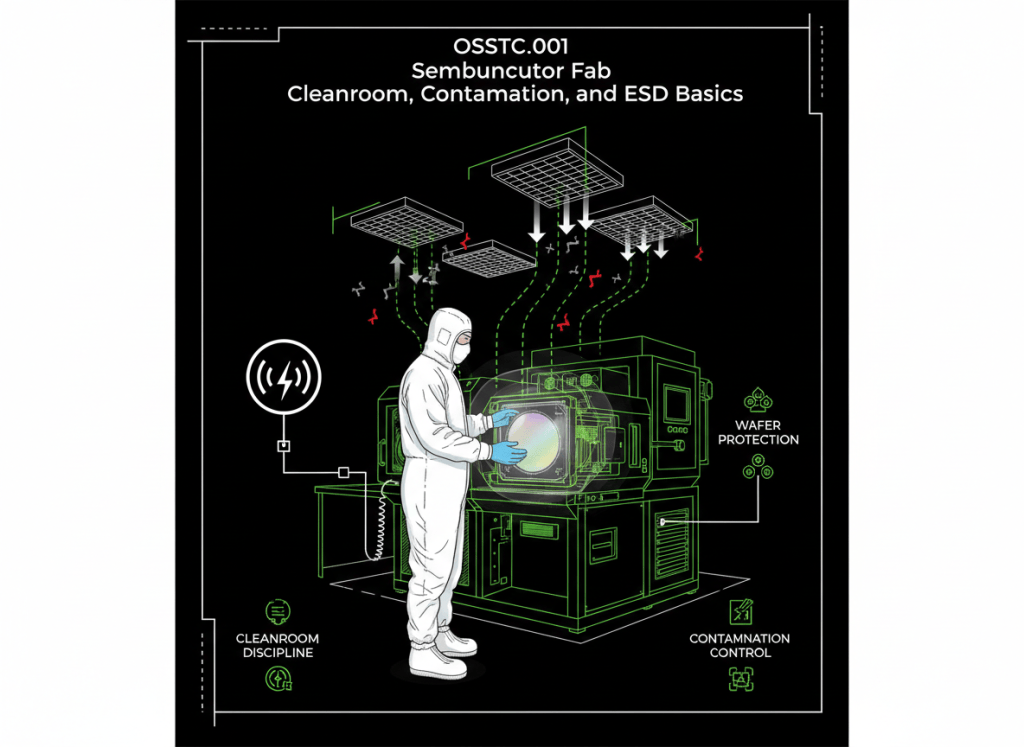
A semiconductor fab is not just a room full of machines. It is a tightly controlled manufacturing environment built to protect wafers from particles, static charge, moisture, chemicals, vibration, and human mistakes.
This is OSSTC.001, the first lesson in the Open Source Semiconductor Technician Certification track. Before learning lithography, etch, deposition, ion implantation, CMP, metrology, or equipment troubleshooting, a technician needs to understand the environment that makes all of those processes possible.
The entire lesson in one picture
People + materials + equipment
↓
can create particles and static
↓
Cleanroom + gowning + filtration + ESD controls
↓
protect the wafer
↓
Higher process stability and fewer avoidable defects
That is the basic technician mindset: protect the process before you touch the process.
What is a semiconductor fab?
A fab, short for fabrication facility, is where semiconductor wafers move through many repeated processing steps until microscopic electronic structures are built on and inside the wafer.
Modern fabs are divided into controlled areas. The cleanroom contains process equipment and wafer-handling systems. Supporting spaces may include sub-fabs, utility areas, chemical-delivery systems, vacuum systems, abatement equipment, electrical distribution, chilled water, exhaust, compressed gases, and many other facility systems.
FAB
Cleanroom → wafer processing tools
Sub-fab → pumps, abatement, support equipment
Utilities → power, gases, water, exhaust, cooling
Support → metrology, maintenance, material handling
A semiconductor technician may work directly on process equipment, support equipment, facilities systems, material handling, or metrology—but the contamination and safety rules still matter across the facility.
Why cleanrooms exist
Semiconductor features are extremely small. A particle that looks invisible to a person can still be large enough to interfere with a process step, block a pattern, scratch a surface, alter a film, or create a defect.
Particle lands on wafer
↓
Process continues
↓
Pattern / film / surface may be disturbed
↓
Defect risk increases
↓
Yield can decrease
Samsung Semiconductor explains that semiconductor cleanrooms are designed to keep dust and particles away from the manufacturing area through controlled airflow and filtration. Its cleanroom overview shows air showers, filtration, and the tightly controlled production environment.
Reference: Samsung Semiconductor — Why semiconductor manufacturing uses cleanrooms.
Video 1: Why semiconductor cleanrooms exist
A cleanroom controls particles—it does not make hazards disappear
One of the easiest beginner mistakes is thinking that “clean” means “safe.” A cleanroom may contain hazardous chemicals, toxic or flammable gases, high voltage, RF energy, hot surfaces, vacuum systems, pressurized lines, moving robots, lasers, and other stored energy.
Cleanroom clothing is primarily contamination-control clothing unless the site specifically rates it as protective equipment for another hazard. A bunny suit does not replace chemical PPE, arc-flash PPE, respiratory protection, lockout/tagout, gas monitoring, or any site-specific safety procedure.
The technician is also a contamination source
People naturally shed particles from skin, hair, clothing, shoes, cosmetics, paper, tools, and ordinary movement. That is why semiconductor cleanrooms use controlled gowning procedures and rules about what can enter the area.
Street environment
↓
Gowning procedure
↓
Controlled garments + footwear + gloves as required
↓
Cleanroom entry
↓
Move and work without creating unnecessary contamination
The exact gowning order is site-specific. Follow the facility’s posted procedure instead of memorizing one universal sequence from the internet.
Cleanroom class: what the number is trying to tell you
Cleanrooms are classified by how many airborne particles of specified sizes are allowed in a defined volume of air. A stricter class means tighter contamination control.
For a technician, the practical lesson is simple: different fab zones can have different cleanliness requirements. Do not assume a procedure permitted in one area is acceptable in another.
Wafer handling: the product is not “just a disk”
A silicon wafer may pass through many tools over a long manufacturing flow. In many modern 300 mm fabs, wafers travel inside a closed carrier called a FOUP—a Front Opening Unified Pod.
FOUP
↓
Tool load port
↓
Automated wafer-handling robot
↓
Process chamber
↓
Wafer returns to carrier
↓
Next tool
The carrier helps isolate wafers from the room environment and allows automated material-handling systems to move lots between tools.
What is ESD?
Electrostatic discharge (ESD) is the transfer of electrostatic charge between objects at different electrical potentials.
A person can accumulate static charge simply by moving, walking, changing garments, or contacting and separating materials. A discharge that is too small for you to feel can still damage sensitive electronics.
Contact / separation of materials
↓
Static charge develops
↓
Potential difference exists
↓
Discharge occurs
↓
Sensitive device may be damaged
The EOS/ESD Association explains that basic ESD control uses grounding, controlled work surfaces, personnel grounding, ionization where appropriate, and verified ESD-control procedures.
Reference: EOS/ESD Association — Basic ESD Control Procedures and Materials.
Video 2: ESD basics for electronics manufacturing
ESD and ESA are related but different
In semiconductor manufacturing, static charge can cause more than direct discharge damage.
- ESD — Electrostatic Discharge: charge transfers suddenly and can damage product or disturb equipment.
- ESA — Electrostatic Attraction: a charged wafer, carrier, reticle, or surface attracts particles that can contaminate the process.
Static charge
ESD → discharge damage / equipment upset
ESA → particles attracted to critical surfaces
SEMI notes that electrostatic charge in wafer fabs can contribute to both ESD and particle attraction. Repeated wafer handling, robotic movement, insulators, carriers, and tool materials can all become part of the static-control problem.
Reference: SEMI — Electrostatic Discharge in Semiconductor Fabrication: Causes and Solutions.
Ground conductors; neutralize charge on insulators
A useful beginner rule is:
Conductive object with unwanted static charge
↓
Proper grounding can provide a controlled path
Insulating object with unwanted static charge
↓
Grounding alone may not remove the charge
↓
Ionization or other approved ESD controls may be needed
This is why a semiconductor fab may use conductive or dissipative floors, approved footwear, grounded work surfaces, grounding points, continuous monitors, ionizers, and other controls depending on the process.
Wrist straps are not the universal answer everywhere
In an electronics bench environment, a wrist strap may be a standard part of personnel grounding. In a semiconductor cleanroom, mobility, garment requirements, process conditions, and tool design can change how personnel grounding is implemented.
Use the site’s approved ESD-control method. Never create your own ground connection, clip onto an unknown point, or assume that a metal frame is an approved grounding point.
Video 3: Where cleanroom rules fit into the manufacturing process
What a technician should check before touching anything
- Am I trained and authorized for this tool or area?
- What contamination-control rules apply here?
- What ESD controls are required?
- Is the product exposed, enclosed in a carrier, or inside the tool?
- What hazardous energies exist? Electrical, pneumatic, hydraulic, vacuum, thermal, RF, chemical, gas, mechanical, or stored energy.
- What PPE is required beyond cleanroom garments?
- Does the procedure require lockout/tagout, a permit, gas monitoring, or another control?
- What condition should the tool be in before I begin?
- What parts, tools, wipes, lubricants, and materials are approved for the cleanroom?
- How will I verify the tool is returned to the correct state when work is complete?
The cleanroom tool rule: approved materials only
Ordinary shop materials can shed particles, outgas, create static, or contaminate surfaces. A cleanroom may control or prohibit items such as cardboard, ordinary paper, pencils, unapproved lubricants, certain plastics, dirty tools, personal electronics, food, cosmetics, and other materials.
Use only the materials approved for the specific fab area and process.
Do not improvise around interlocks
Semiconductor equipment can contain multiple safety interlocks. An interlock may prevent access to hazardous voltage, lasers, moving mechanisms, RF power, process gases, vacuum, or other hazards.
Never defeat, tape down, bypass, spoof, or hold an interlock closed just to make a tool run. If an approved maintenance procedure requires an interlock override, that procedure belongs to qualified and authorized personnel using the manufacturer’s and site’s documented method.
A simple contamination troubleshooting example
Imagine a tool begins showing an increase in particle-related defects.
Particle trend rises
↓
Do not immediately replace random parts
↓
Check process history and alarms
↓
Check maintenance activity
↓
Check approved cleaning state
↓
Check wafer / carrier handling
↓
Check airflow / filtration / tool condition as authorized
↓
Use data to isolate the source
A technician’s job is not to guess. It is to preserve evidence, follow the troubleshooting procedure, and make controlled changes one step at a time.
A simple ESD troubleshooting example
Suppose an ESD monitor or workstation check fails.
ESD control check fails
↓
Stop handling exposed ESD-sensitive product
↓
Verify approved grounding / monitor setup
↓
Check required footwear / wrist strap / mat / connections
↓
Correct the control problem
↓
Re-verify before resuming work
Do not continue handling sensitive product just because “it worked yesterday.” ESD controls must work now.
Common beginner mistakes
- Thinking a cleanroom suit automatically protects against every fab hazard.
- Touching wafers, reticles, carriers, connectors, or sensitive parts without knowing the handling rule.
- Bringing unapproved materials into a clean area.
- Assuming a tiny particle cannot matter because you cannot see it.
- Assuming you must feel a static shock before ESD can damage electronics.
- Using an arbitrary metal surface as an ESD ground.
- Ignoring failed ESD-monitor or grounding checks.
- Opening a tool because the process chamber “looks idle.”
- Bypassing an interlock to save time.
- Making several troubleshooting changes at once and losing the cause/effect trail.
Practice exercise: read the fab like a technician
For each situation, identify the first thing you should think about.
- You are handed an unbagged tool from a regular workshop and asked to bring it into the cleanroom.
- An ESD monitor shows a fault while exposed electronics are on the bench.
- You see a wafer carrier sitting outside its normal location.
- A tool is idle but the vacuum pump is still running.
- A technician wants to bypass a door interlock to “just check one thing.”
- A particle alarm appears immediately after preventive maintenance.
Good technician answers: verify cleanroom approval before bringing the tool in; stop exposed-product handling until ESD controls are restored; follow material-handling procedure for the carrier; treat running vacuum equipment as energized until the procedure proves otherwise; do not bypass the interlock without an authorized procedure; and correlate the particle event with the maintenance history before guessing.
Knowledge check
1. Why are semiconductor wafers processed in cleanrooms?
To control particles and other contamination that can create defects and reduce process yield.
2. What is ESD?
The transfer of electrostatic charge between objects at different electrical potentials.
3. What is ESA?
Electrostatic attraction—the attraction of particles or materials to a charged surface.
4. Does a cleanroom bunny suit replace hazard-specific PPE?
No. Cleanroom garments are primarily contamination-control garments unless specifically rated for another hazard.
5. Why should a technician care about a failed ESD control even if no visible spark occurs?
ESD-sensitive product can be damaged by discharges too small for a person to feel.
6. What is the safest response to an unknown fab condition?
Stop, identify the hazard and procedure, verify authorization, and use controlled troubleshooting instead of improvising.
Key takeaway
A semiconductor technician protects three things at the same time: people, product, and process. Cleanroom discipline protects the wafer from contamination. ESD controls protect sensitive product and equipment from static effects. Safety procedures protect people from the very real electrical, chemical, mechanical, vacuum, thermal, and gas hazards inside a fab.
PEOPLE → safety procedures
PRODUCT → cleanroom + ESD control
PROCESS → disciplined, documented work
All three matter.
Display note: all diagrams in this lesson are plain educational diagrams, not simulated terminals. No VS Code, Windows, or Linux terminal palette is being represented or invented.
BitcoinVersus.Tech
Advertisement
Editor’s Note:
We volunteer daily to ensure the credibility of the information on this platform is Verifiably True. If you would like to support our research initiatives, please donate here: 3C9o19EH5HSiwEPyCTmEKzxhNCbo2X6TTb
BitcoinVersus.tech is not a financial advisor. This media platform reports on financial subjects purely for informational purposes.


Leave a Reply