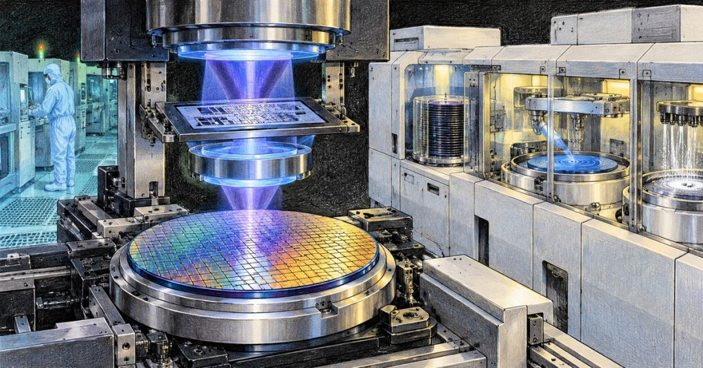
Photolithography is the pattern-transfer step that lets a semiconductor fab place microscopic circuit features onto a wafer. A technician does not need to redesign the optical system, but does need to understand the equipment chain, wafer flow, alignment logic, focus control, contamination risks, alarms, and the difference between a scanner fault and a track-process fault.
ASML gives a short overview of the lithography systems used to manufacture modern microchips.
This lesson follows OSSTC.008: Semiconductor Metrology and Inspection Basics. Metrology measures whether a pattern was printed correctly; photolithography equipment is the machinery that coats, aligns, exposes, develops, and transports the wafer so that pattern can be created in the first place.
Learning Objectives
- Identify the major modules in a photolithography cell.
- Explain the purpose of photoresist coat, bake, alignment, exposure, post-exposure bake, and develop.
- Distinguish the coat/develop track from the scanner or stepper.
- Explain wafer alignment, leveling, focus, overlay, and exposure dose at a technician level.
- Recognize common equipment symptoms and perform safe first-line fault isolation.
- Connect lithography faults to metrology and defect data without changing recipes casually.
The Lithography Cell
A production lithography cell normally combines two major equipment groups: a coat/develop track and a lithography exposure system. The track applies and processes photoresist; the scanner or stepper aligns the wafer to the reticle pattern and exposes the resist with controlled light. Wafers move between these modules under recipe control, and a fault in either side can create similar downstream symptoms.
ASML Nanoland explains the wafer-to-chip manufacturing flow and where photolithography fits into the process.
Coat, Bake, Expose, Develop
The basic sequence is: surface preparation, resist dispense and spin coating, soft bake, wafer alignment, exposure, post-exposure bake where required, development, rinse, and inspection or metrology. Tokyo Electron describes modern CLEAN TRACK systems as 300 mm coater/developer platforms built for high-volume lithography processes, including advanced immersion and EUV process flows. For technicians, stable chemical delivery, chuck condition, dispense position, spin control, bake temperature, exhaust, wafer handling, and module cleanliness are all part of keeping the track repeatable.
Branch Education provides a detailed walk-through of EUV lithography, including reticles, optics, wafer transport, wafer alignment, and photoresist.
Reticle, Optics, and Exposure
The reticle contains the pattern to be printed. In DUV systems, lenses form and reduce the optical image; in EUV systems, multilayer mirrors guide and focus 13.5 nm light because EUV is strongly absorbed by ordinary materials and air. The exposure system controls illumination, projection optics, wafer-stage motion, reticle-stage motion, and dose so the intended pattern reaches the resist at the correct scale and location.
Huygens Optics explains diffraction, imaging, masks, critical dimension, and computational corrections used in advanced lithography.
Alignment, Leveling, Focus, and Overlay
Before exposure, the scanner must determine where the wafer actually is. Alignment sensors read special wafer marks, while leveling sensors map wafer height and surface shape so the stage can position the wafer inside the usable focus window. Overlay is the layer-to-layer placement error; focus describes whether the projected image is sharp at the resist plane. These variables are related but not interchangeable, and both are monitored by the metrology systems covered in OSSTC.008.
ASML shows wafer loading, alignment markers, leveling, electrostatic clamping, and precision stage motion in a High-NA EUV system.
What Technicians Watch
Technician work centers on equipment state and repeatability: FOUP identity, wafer presence, robot transfer, vacuum or environmental readiness, chuck and stage condition, sensor status, chemical and utility availability, temperature stability, module alarms, interlocks, contamination control, and whether the recipe loaded is the authorized one. A technician should preserve logs and raw evidence before resetting faults, and should not modify process setpoints merely to make an alarm disappear.
ASML shows cleanroom assembly, technical training, quality control, and the technician environment surrounding complex lithography equipment.
Common Symptom Patterns
- Wafer transfer fault: check wafer presence sensing, robot path, end effector condition, FOUP position, vacuum grip, mechanical interference, and upstream/downstream readiness.
- Alignment failure: verify the correct wafer and recipe, mark visibility, contamination, wafer orientation, stage condition, and whether the failure is isolated to one wafer or repeats across the lot.
- Focus or leveling excursion: inspect chuck cleanliness, wafer backside contamination, wafer bow/warp evidence, leveling-sensor alarms, temperature stability, and metrology results.
- Track coat defect: inspect dispense behavior, nozzle condition, spin chuck cleanliness, resist supply, exhaust, wafer centering, and recent maintenance history.
- Bake-related drift: compare hotplate temperature checks, stabilization time, wafer contact, recipe identity, and lot history.
- Overlay shift: compare alignment performance, scanner state, wafer geometry, process history, and overlay metrology before assuming a single hardware cause.
A Safe Troubleshooting Order
- Confirm wafer, lot, layer, recipe, reticle, and tool identity.
- Record the exact alarm, timestamp, module, wafer position, and sequence step.
- Determine whether the issue affects one wafer, one lot, one module, or multiple tools.
- Check utilities, interlocks, sensors, transfer status, and recent maintenance events.
- Inspect only technician-authorized contamination-sensitive surfaces and handling hardware.
- Compare the failure with known-good logs, metrology, wafer maps, and matched-tool behavior.
- Repeat only approved recovery procedures; do not bypass safety interlocks or alter qualified process values.
- Escalate with preserved logs, screenshots, wafer IDs, alarm history, and the checks already completed.
Lithography Data Connects Back to Metrology
ASML describes lithography control as a closed feedback problem: sensors inside the scanner and external metrology systems measure focus, overlay, pattern placement, and other variables, then corrections are applied to improve subsequent exposures. KLA similarly describes overlay metrology as feedback for lithography control. This is why technicians should preserve metrology context instead of treating an exposure tool alarm as an isolated mechanical event.
ASML provides an additional view of High-NA wafer-stage operation and the precision motion needed during exposure.
Industry Context
Advanced lithography equipment is unusually complex because optical, vacuum, motion-control, thermal, sensing, software, contamination, and process-control systems must all work together. The social post below is included as industry commentary on that complexity; the technical claims in this lesson are grounded in the primary manufacturer references listed later.
Hands-On Exercise
Draw a simplified lithography cell with these blocks in order: FOUP load port, track robot, coat module, soft bake, scanner, post-exposure bake, develop, rinse/dry, and metrology. Mark which steps are mainly mechanical, chemical, thermal, optical, or measurement-driven.
Then build a fault-isolation table for three symptoms: alignment failure, edge coating defect, and repeated focus excursion. For each symptom, list five observations to collect before changing any hardware or recipe value.
Knowledge Check
- What is the difference between a coat/develop track and a lithography scanner?
- Why is photoresist used?
- What does the reticle contain?
- Why does the scanner perform wafer alignment before exposure?
- What is the difference between focus and overlay?
- Name three equipment causes that can contribute to a focus or leveling problem.
- Why should technicians preserve logs before resetting a fault?
- Why should a qualified recipe not be changed casually during troubleshooting?
Answers
- The track coats, bakes, develops, and handles the resist process; the scanner or stepper aligns and exposes the wafer pattern.
- It is a light-sensitive layer that records the projected pattern so later process steps can selectively modify the wafer.
- The circuit-layer pattern or mask information to be projected onto the wafer.
- It must determine the wafer’s actual position relative to alignment marks so the new layer is placed correctly.
- Focus is image sharpness at the resist plane; overlay is the placement error between patterned layers.
- Examples include chuck contamination, backside particles, wafer bow or warp, leveling-sensor problems, temperature instability, or stage-related faults.
- Resetting can erase transient evidence and make intermittent faults harder to diagnose.
- Changing a qualified parameter can create new process variation, hide the original cause, and invalidate comparisons with known-good production data.
Previous Related Lessons
- OSSTC.008: Semiconductor Metrology and Inspection Basics
- OSSTC.007: Wafer Probe Testing
- OSSTC.003: Semiconductor Vacuum Systems
- OSSTC.002: Wafer Handling, FOUPs, and Automated Material Flow Basics
- OSSTC.001: Semiconductor Fab Cleanroom, Contamination, and ESD Basics
Related BitcoinVersus.Tech Reading
- What Is Photoresist?
- ASML and ZEISS Map Hyper-NA EUV to 5 nm Half-Pitch
- Gigaphoton Says It Can Recycle 50% of the Neon Used in Chip Lithography
Primary references: ASML — Lithography Principles, ASML — How Microchips Are Made, ASML — Measuring Accuracy, ASML — Aligning Lithography to the Nanometer, Tokyo Electron — CLEAN TRACK LITHIUS Series, and KLA — Semiconductor Metrology.
BitcoinVersus.Tech Editor’s Note:
We volunteer daily to ensure the credibility of the information on this platform is Verifiably True. If you would like to support to help further secure the integrity of our research initiatives, please donate using the QR code provided
For best QR-code scanning results, please scan this donation code from a desktop or larger screen. Mobile screens may prevent camera recognition.
BitcoinVersus.Tech provides technical education and analysis for informational purposes only.


Leave a Reply