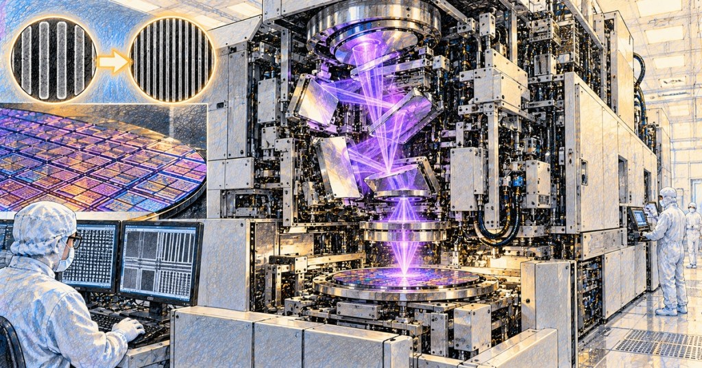
ASML and ZEISS are already sketching the machine that could come after today’s High-NA EUV era. A new peer-reviewed paper describes a Hyper-NA lithography system with a numerical aperture of at least 0.75, up from the 0.55 NA used by current High-NA EUV scanners. The goal is roughly 5 nm half-pitch resolution, versus about 8 nm for today’s High-NA generation.
The development matters because High-NA EUV has only just moved into chip production, yet the semiconductor industry is already planning the next optical step. Reuters reports that ASML has begun development work on Hyper-NA but has not committed to producing a commercial system; engineers from ASML and optical partner Carl Zeiss say the technology could be ready in roughly a decade if the remaining technical and economic problems are solved.
Hyper-NA Pushes Numerical Aperture Past 0.55
In lithography, numerical aperture is one of the main levers that determines how finely an optical system can resolve patterns. ASML’s current High-NA EUV platform raises NA from the earlier 0.33 generation to 0.55. Hyper-NA would push that to at least 0.75.
The new paper, summarized by Semiconductor Engineering, examines how that jump could extend EUV patterning while keeping much of the existing ecosystem intact. The authors focus on optical architecture, reticle 3D effects, polarization at the wafer, and the practical limits of building larger projection mirrors without making the scanner dramatically larger.
The Target Is About 5 nm Half-Pitch
The most important number in the paper is not a marketing node name. It is the physical patterning target. The researchers describe Hyper-NA as a path toward roughly 5 nm half-pitch, compared with about 8 nm for current EXE-class High-NA systems and roughly 13 nm for older NXE-class EUV tools.
That does not mean “5 nm chips” in the way consumer processors are marketed. Semiconductor node names are no longer literal measurements of one transistor feature. Half-pitch is a lithography resolution metric tied to the spacing of repeated structures. The advantage is still real: finer printable structures can help chipmakers pack more logic and memory into a given area and reduce the number of multi-patterning steps needed for critical layers.
ASML Wants to Reuse as Much of EUV as Possible
One reason Hyper-NA is credible is that the proposal does not throw away the entire EUV stack. Reuters says the new machine could reuse much of the existing light-source technology, while ZEISS is already capable of manufacturing the ultra-precise mirrors needed for the next optical generation. The researchers also argue that the machine footprint would grow only modestly even though the mirrors themselves become significantly larger.
That reuse is economically important. EUV systems are among the most complex industrial machines ever built, and every new optical generation forces changes across the photoresist, mask, metrology, inspection, process-control, and wafer-handling ecosystem. The closer Hyper-NA can stay to existing EUV infrastructure, the easier it becomes for fabs to justify adoption.
ASML has also shown the current High-NA platform in an official LinkedIn walkthrough, illustrating the EUV light source, anamorphic optics, reticle path, and wafer exposure system that Hyper-NA would build on.
Reticles and Polarization Become Harder at Higher NA
Higher numerical aperture does not arrive for free. The paper identifies two major problem areas: 3D effects at the reticle and polarization effects at the wafer. As the optical angles become more extreme, features on the mask can influence imaging in ways that are less important at lower NA, while polarization behavior can change the contrast and fidelity of the printed pattern.
BitcoinVersus.Tech has already covered one High-NA side effect: ASML and TSMC are studying larger photomasks to work around High-NA’s half-field limitation. Hyper-NA pushes that same design philosophy further. The scanner, reticle, optics, resist, inspection tools, and process recipes have to evolve together.
High-NA Is Still the Near-Term Roadmap
Hyper-NA is not about replacing High-NA next year. High-NA is still the immediate production transition. Reuters says Intel has already adopted High-NA in production, while Samsung and SK Hynix are expected to follow around 2028 and TSMC around 2030. That adoption curve gives the industry years to learn how 0.55 NA behaves in high-volume manufacturing before deciding whether 0.75-plus NA makes economic sense.
This is a familiar semiconductor pattern. Toolmakers develop the next generation while customers are still ramping the current one. The same long planning horizon appears across atomic-scale deposition, advanced packaging, plasma etching, and metrology because every process step has to remain aligned as transistor dimensions shrink.
Why AI Keeps Pulling Lithography Forward
The most important commercial pressure behind this roadmap is AI. Leading accelerators combine enormous logic die, dense cache, advanced packaging, and high-bandwidth-memory packaging. More compute per watt requires improvements at every layer: transistor density, interconnect, memory bandwidth, packaging, cooling, and power delivery.
TSMC has been describing AI as a long-term foundry growth driver since at least 2024. That demand is now pulling not only wafer capacity but also lithography and advanced packaging capacity forward. Finer patterning does not solve the entire AI scaling problem, but it remains one of the core tools for increasing useful compute density.
The Economics May Decide Whether Hyper-NA Ships
ASML can prove that Hyper-NA is technically possible and still decide not to build it at scale. The final decision will depend on cost per wafer, throughput, uptime, mask and resist readiness, yield, and whether the tool saves enough process steps to justify the capital expense. Wafer yield matters because finer resolution is only valuable if fabs can print it repeatedly across thousands of wafers with acceptable defect density.
The Reuters report says ASML has started development but has not committed to commercial production. That distinction matters. Hyper-NA is a roadmap technology, not yet a purchase order.
What Comes After Hyper-NA?
Hyper-NA may also mark the practical upper end of today’s 13.5 nm EUV wavelength. The paper suggests that pushing substantially beyond it could require a shorter light wavelength or an entirely different patterning approach. Research groups and startups are already exploring those possibilities, but they are much less mature than the path from 0.55 to 0.75-plus NA.
For now, the semiconductor roadmap remains evolutionary: make High-NA work, improve the resist and mask ecosystem around it, learn from high-volume production, then decide whether Hyper-NA can deliver enough additional shrink to pay for another generation of extraordinarily complex optics.
BitcoinVersus.Tech
Advertisement
BitcoinVersus.Tech covers semiconductors, AI hardware, data centers, chip manufacturing, software, networking, and the infrastructure behind modern computing.
Editor’s Note
Primary reporting for the current Hyper-NA roadmap comes from Reuters and the October 2026 peer-reviewed technical paper by researchers from Carl Zeiss SMT and ASML. Hyper-NA remains a development roadmap, not a committed commercial production system.
We volunteer daily to help keep the information on this platform verifiably accurate. Support our independent research through the support options available on BitcoinVersus.Tech.
BitcoinVersus.tech is not a financial advisor. Content is provided for informational purposes.


Leave a comment