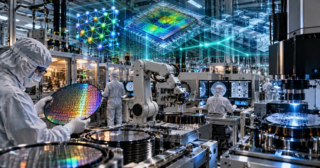
NVIDIA is pushing its accelerated-computing stack deeper into the semiconductor factory itself. At SEMICON West on October 14, 2026, the company announced an expanded set of CUDA-X and Omniverse tools aimed at chip design, process simulation, inspection, digital twins, and what NVIDIA calls the AI-defined fab: a semiconductor factory where AI helps engineers model materials, test process changes, inspect wafers, optimize operations, and automate more of the engineering loop.
The most notable new software component is NVIDIA cuPotential, a new CUDA-X library designed to help developers build AI agents that simulate how atoms and molecules interact. NVIDIA says early-access testing shows cuPotential can accelerate workflows that were already GPU-optimized by an additional 2–3×. That number comes from NVIDIA’s own early testing, so it should be treated as a vendor-reported result rather than an independently reproduced benchmark.
NVIDIA AI Infrastructure’s official SEMICON West post highlights semiconductor manufacturing, physical AI, robotics, fab digital twins, and accelerated computing sessions scheduled for October 14.
Why AI is moving into the fab
Modern chip manufacturing is already one of the most data-intensive industrial processes on Earth. A leading fab must control lithography, deposition, etch, cleaning, metrology, inspection, packaging, equipment maintenance, scheduling, and thousands of process parameters while keeping defects extremely low. Every smaller geometry makes that control problem harder.
Many of the physical steps are familiar to BitcoinVersus.Tech readers. Photoresist and photolithography transfer patterns onto the wafer, while plasma and wet etching selectively remove material. At advanced nodes, even a small modeling error, process drift, overlay issue, contaminant, or inspection miss can affect yield across a large number of expensive wafers.
The traditional response is more simulation, more metrology, tighter process control, and more engineering analysis. NVIDIA’s pitch is that AI agents and GPU acceleration can shorten those loops: simulate a process before running it, analyze large inspection images faster, build digital twins of equipment or entire factories, and let software agents search a larger engineering design space before a human commits an expensive physical experiment.
NVIDIA Omniverse’s official GTC 2026 session with Samsung and Synopsys shows how agentic AI, computational lithography, digital twins, and closed-loop fab simulation are being applied to semiconductor manufacturing.
cuPotential goes down to atoms and molecules
cuPotential is aimed at a lower layer of the manufacturing problem: atomic and molecular interaction. Semiconductor materials engineering often requires simulations that estimate how atoms behave under different structures, materials, temperatures, fields, or process conditions. These calculations can be expensive even before an AI agent begins exploring thousands of possible variations.
NVIDIA says cuPotential gives AI agents an accelerated physics layer for those searches. Rather than an agent merely generating text or recommending a process change, the intended workflow is closer to an engineering loop: propose a candidate, run an accelerated simulation, evaluate the result, then iterate.
That distinction matters. An AI agent that cannot interrogate physics is limited to patterns found in its training data and available engineering records. An agent connected to a validated simulation tool can test a proposed material or process configuration against a computational model before an engineer considers a physical wafer run. The quality of the outcome still depends on the accuracy of that physical model, the training data, and the engineer’s validation.
Lam Research reports 30× faster simulation with NanoVDB
NVIDIA also highlighted NanoVDB, its open-source library for compact GPU processing of sparse three-dimensional volumetric data. According to NVIDIA, Lam Research has used NanoVDB to accelerate semiconductor manufacturing simulation by as much as 30×.
Three-dimensional process simulation is important because a wafer is not just a flat drawing. Deposition, etching, conformality, sidewall geometry, trenches, vias, and other structures develop in three dimensions. The more accurately engineers can simulate those shapes and interactions before running equipment, the more process variants they can evaluate without consuming wafer starts and tool time.
Again, the 30× figure is a company-reported result cited by NVIDIA. The announcement does not provide enough public methodology to treat it as a universal speedup for all Lam workloads. The important technical point is that sparse 3D data processing is becoming another workload that semiconductor equipment companies can move onto GPUs.
NVIDIA AI Infrastructure previously documented TSMC’s adoption of CUDA-X, Metropolis, TAO Toolkit, and Omniverse for chip design, fab operations, and defect detection, showing the broader manufacturing direction behind the new SEMICON West announcement.
KLA is applying GPU image processing to inspection
Inspection is another obvious target for accelerated computing. Semiconductor inspection systems can produce enormous image datasets while looking for particles, pattern defects, line-edge irregularities, scratches, missing material, and other anomalies. NVIDIA says KLA is using NVIDIA Performance Primitives, or NPP, to accelerate image-processing workloads used in semiconductor inspection.
That does not mean an AI system simply decides whether a wafer is good or bad. Inspection normally combines optics, sensors, deterministic image processing, statistical methods, classification systems, equipment-specific algorithms, and human engineering judgment. The GPU’s role is to accelerate parts of that pipeline so more data can be processed within the manufacturing cycle time.
The same logic applies to advanced lithography. BitcoinVersus.Tech recently covered how ASML and ZEISS are mapping Hyper-NA EUV toward a 5 nm half-pitch. As optical systems, masks, resist behavior, and correction algorithms become more complex, the amount of computation required before exposure keeps increasing. Accelerated computing is increasingly part of the manufacturing toolchain rather than something that begins only after a chip leaves the fab.
Digital twins move from visualization toward engineering
NVIDIA is also positioning Omniverse libraries as infrastructure for semiconductor digital twins. A digital twin can represent an individual tool, a production cell, material flow, or an entire factory. In the semiconductor context, engineers can use those models to test layout changes, maintenance procedures, robot paths, throughput constraints, or process interactions before disrupting physical production.
The idea becomes more consequential when AI agents are connected to the twin. Instead of a static model that a human manually interrogates, an agent can potentially propose multiple scheduling or process scenarios, simulate them, compare outcomes, and surface promising candidates for engineering review.
NVIDIA’s SEMICON West program reflects that shift. Sessions on October 14 included physical AI in the fab, robotics, real-time process digital twins, computational lithography, and semiconductor manufacturing with speakers or participants from TSMC, Applied Materials, Lam Research, Tokyo Electron, Micron, Siemens, FANUC, and Universal Robots.
NVIDIA AI Infrastructure’s official Samsung post shows the same concept at factory scale: an AI factory architecture aimed at semiconductor manufacturing and more autonomous fab operations.
What NVIDIA has actually announced — and what it has not
The strongest evidence in this announcement is technical adoption: major semiconductor design, equipment, inspection, and manufacturing companies are integrating NVIDIA libraries into real engineering workflows. The announcement names Applied Materials, Cadence, KLA, Lam Research, Siemens, Synopsys, and others, while NVIDIA’s SEMICON West program includes additional manufacturers and automation companies.
What the announcement does not establish is a universal fab-level productivity gain. NVIDIA does not publish a single percentage showing that an “AI-defined fab” automatically produces more good wafers, cuts cycle time by a fixed amount, or improves yield by a specific number. Individual speedups such as 2–3× for cuPotential early-access workflows or 30× for a Lam simulation are workload-specific and should not be generalized to an entire semiconductor factory.
There are also practical limits. Semiconductor production is governed by strict process qualification, statistical process control, equipment certification, recipe control, safety rules, and customer requirements. A generative model cannot simply rewrite a production recipe and push it into a high-volume manufacturing tool. The more realistic near-term role for AI agents is to accelerate analysis, simulation, troubleshooting, optimization, and engineering decision support while validated control systems remain in charge of physical production.
The semiconductor industry is becoming its own AI customer
The circularity of this trend is notable. Semiconductor companies manufacture the chips that make modern AI possible. Those same companies are now consuming increasingly large amounts of accelerated computing to design the next chips, simulate the processes that manufacture them, inspect wafers, optimize factories, and coordinate robots and equipment.
That means the AI hardware race is no longer only about data centers running language models. It is also moving upstream into the factories that determine how quickly new processors can be designed and manufactured. If the tools become reliable enough, the competitive advantage may come partly from shortening the loop between a proposed physical change, its simulated result, its measured wafer result, and the next engineering iteration.
For now, the most defensible conclusion is narrower: NVIDIA is expanding the set of semiconductor workflows that can run on GPUs and be exposed to AI agents. The company has concrete partner examples in atomistic simulation, three-dimensional process modeling, inspection, computational lithography, and digital twins. Whether those tools ultimately produce measurable fab-wide yield and productivity improvements will require more detailed production data and independent validation.
BitcoinVersus.Tech Editor’s Note:
We volunteer daily to ensure the credibility of the information on this platform is Verifiably True. If you would like to support to help further secure the integrity of our research initiatives, please donate using the QR code provided

For best QR-code scanning results, please scan this donation code from a desktop or larger screen. Mobile screens may prevent camera recognition.


Leave a Reply