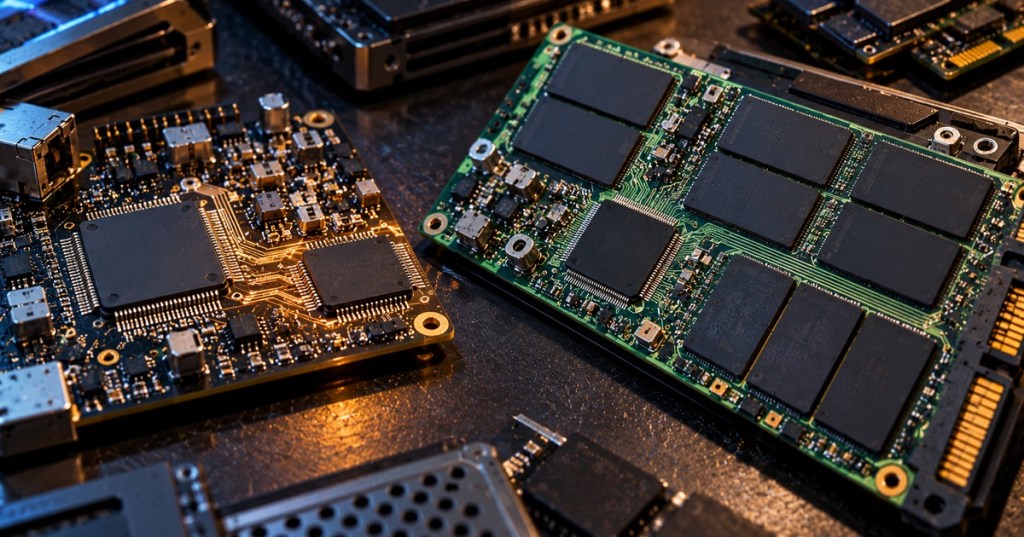
NAND and NOR are the two major families of flash memory, but they are optimized for very different jobs. NOR is built for fast random reads and direct code execution. NAND is built for high density, large sequential transfers and low cost per bit. That is why NOR commonly stores boot code and firmware while NAND dominates SSDs, memory cards, phones and high-capacity embedded storage.
Both are nonvolatile: unlike the technologies in our SRAM vs DRAM comparison, NAND and NOR retain data after power is removed. But their cell organization, interfaces and access patterns create very different performance characteristics.
| Category | NOR Flash | NAND Flash |
|---|---|---|
| Primary strength | Fast random reads and code execution | High density and low cost per bit |
| Typical use | Firmware, bootloaders, embedded code | SSDs, phones, memory cards, bulk storage |
| Read access | Random, byte/word oriented | Page oriented |
| Execute in place | Common | Usually no |
| Density | Lower | Much higher |
| Write/erase handling | Relatively simple at small scale | Controller-managed pages and blocks |
| Cost per bit | Higher | Lower |
Why They Are Called NOR and NAND
The names come from how the memory cells are electrically connected. NOR flash arranges cells in a structure resembling a NOR logic gate, allowing individual locations to be addressed more directly. NAND strings multiple cells together in series, resembling NAND logic. That serial organization reduces wiring and silicon overhead, which is one reason NAND can reach much higher densities.
Both technologies commonly store charge in floating-gate or charge-trap structures. Programming and erasing change the electrical state of the cell, and the memory senses that state later to reconstruct the stored bits. Unlike SRAM or DRAM, that state can remain for years without continuous power.
NOR: Built for Direct Access
NOR flash is valuable when a processor needs dependable, low-latency access to relatively small amounts of code. Its random-read behavior allows a CPU or microcontroller to fetch instructions directly from the flash device rather than copying an entire image into RAM first.
That capability is called execute in place, or XIP. Infineon’s NOR flash documentation identifies fast random access and direct code execution as core reasons NOR is used for boot code, embedded firmware, automotive ECUs and industrial control systems.
Serial NOR devices using SPI, QSPI or newer high-speed interfaces are especially common on embedded boards. A small flash package can hold the first-stage bootloader, device configuration and application firmware while a microcontroller or SoC starts directly from that image.
NAND: Built for Capacity
NAND trades direct byte-style access for far greater density. Data is typically read and written in pages, while erase operations happen across much larger blocks. The memory therefore works best when a controller can manage the difference between the logical data requested by software and the physical pages and blocks inside the flash array.
Micron’s NAND documentation shows how modern TLC NAND is aimed at high-capacity storage across PCs, mobile devices, vehicles, data centers and cloud systems. NAND can also store multiple bits in each cell—SLC, MLC, TLC and QLC trade endurance and programming margin for still greater density.
English translation: SK hynix is a major memory-chip manufacturer producing DRAM, NAND flash and HBM for systems including AI servers and data centers.
The Controller Changes Everything
Raw NAND is not used like normal RAM. A storage controller must account for bad blocks, error correction, erase-before-write behavior, wear, page placement and background cleanup. SSD controllers translate operating-system reads and writes into the physical operations the NAND array can perform.
This translation layer is why an SSD can present a clean block-device interface even though the underlying flash cannot simply overwrite arbitrary bytes in place. Our guide to NAND, SSD controllers and DRAM cache explains how the controller, flash translation layer and cache work together.
Erase Blocks and Write Amplification
Flash cells must be erased before they can be programmed into a new state. NAND complicates that because erase granularity is much larger than write granularity. A drive may write a page but need to erase an entire block before reclaiming the space later.
That creates garbage collection and write amplification. If valid and invalid pages share the same erase block, the controller may copy useful data elsewhere, erase the block and then reuse it. Better firmware tries to minimize those internal movements because every extra program/erase cycle consumes time, energy and endurance.
Why NOR Is Still Essential
NAND’s enormous density does not make NOR obsolete. A system still needs a reliable place to begin execution. Motherboards, routers, industrial controllers, vehicles and embedded devices often keep boot code or recovery firmware in NOR because it can be addressed directly and validated before larger storage devices are initialized.
This is also why firmware recovery procedures treat flash carefully. Corrupting boot code can prevent a device from reaching the software required to repair itself. Our firmware flashing and bootloader guide covers that operational side of nonvolatile memory.
Where NAND Wins Completely
For terabytes of storage, NAND’s density advantage is overwhelming. An SSD, smartphone or memory card must store huge amounts of data at a cost users can tolerate. NAND arrays can scale vertically through 3D stacking and horizontally across many packages and channels, while controllers parallelize operations to reach very high aggregate throughput.
That makes NAND a storage technology rather than a direct substitute for NOR firmware memory. High-capacity NAND increasingly sits behind sophisticated controllers, ECC engines, DRAM or SRAM caches, PCIe interfaces and NVMe command queues. What software sees as a simple logical drive is actually a large distributed flash-management system.
Endurance Is a System Property
Flash cells wear as program/erase cycles accumulate, but endurance cannot be judged by cell type alone. SLC generally tolerates more cycling than TLC or QLC because it stores fewer voltage states per cell, but controllers can extend practical drive life through wear leveling, spare area, ECC and workload management.
NOR also has endurance limits, especially when firmware or small configuration regions are updated repeatedly. Designers therefore choose the memory technology, density, interface and expected write pattern together rather than assuming one flash family is automatically more durable.
Which One Wins?
- Fast random code reads: NOR.
- Execute in place: NOR.
- Boot firmware: NOR.
- Highest density: NAND.
- Lowest cost per bit: NAND.
- SSDs and bulk storage: NAND.
- Real embedded systems: often both.
Bottom Line
NOR is optimized to make code available quickly and directly. NAND is optimized to store enormous amounts of data economically. The difference is not simply that one is “faster” and the other is “bigger.” Their architectures lead to different access models, erase behavior, controller requirements and system roles. Modern electronics often use NOR to start the machine and NAND to hold everything the machine needs after it starts.
BitcoinVersus.Tech Editor’s Note:
We volunteer daily to ensure the credibility of the information on this platform is Verifiably True. If you would like to support to help further secure the integrity of our research initiatives, please donate using the QR code provided

For best QR-code scanning results, please scan this donation code from a desktop or larger screen. Mobile screens may prevent camera recognition.


Leave a Reply