Semiconductor etching is the process of selectively removing material from a wafer to create the tiny holes, trenches, lines, contacts, gates, and other structures that eventually become a working chip. If photoresist tells the fab where a pattern should go, etching is one of the main processes that actually cuts that pattern into the material underneath.
The easiest way to remember it is simple: deposition adds material; etching removes material. Modern semiconductor manufacturing repeats both operations many times across a 300 mm silicon wafer while lithography keeps telling the process tools exactly where each new structure belongs.
Etching Turns a Lithography Pattern Into a Physical Structure
The patterning flow usually begins with a layer already present on the wafer: silicon, silicon dioxide, silicon nitride, a metal, or another semiconductor material. The wafer is coated with light-sensitive photoresist, exposed through a photomask or reticle, and developed so part of the underlying layer is protected while another part is left open.
The etch tool then removes material from the unprotected regions. Applied Materials describes etching as the selective removal of material from the wafer surface so additional structures can be created or new materials can later be deposited.
After the etch is complete, the temporary masking material can be stripped away. The wafer now contains a permanent physical feature that mirrors the pattern created by lithography.
Wet Etching Uses Liquid Chemistry
Wet etching uses a liquid chemical solution that reacts with the target material. Depending on the chemistry, the liquid may attack silicon, oxide, metal, or another film while leaving neighboring materials relatively untouched.
Wet etching can be highly selective, meaning the chemistry removes one material much faster than another. But it is often isotropic: the reaction can move sideways as well as downward. That makes wet processes useful for many cleaning and removal steps, but less ideal when a fab needs extremely vertical sidewalls.
Lam Research explains that wet etching commonly relies on chemical reactions in liquid solutions and can have limited control over the final shape compared with advanced dry etch processes.
Dry Etching Uses Gases and Plasma
Dry etching replaces the liquid bath with gases inside a low-pressure process chamber. In many advanced steps, radio-frequency energy turns those gases into plasma, a mixture containing charged ions, electrons, and highly reactive neutral species.
The chemistry reacts with exposed material while electrically accelerated ions can strike the wafer in a controlled direction. That combination allows the process to remove material more vertically than a purely isotropic liquid reaction.
Lam calls reactive ion etching, or RIE, a primary semiconductor etch technology. The company explains that charged ions activate the wafer surface and help form features ranging from transistor structures to deep, narrow holes used in memory and 3D semiconductor packaging.
Why Directionality Matters
Imagine trying to cut a narrow trench straight down through a material stack. If the etch also removes too much material sideways, the opening widens and the final dimensions no longer match the design.
A directional, or anisotropic, etch removes material primarily downward. That makes it possible to create narrow trenches, contacts, vias, transistor features, and other structures with much straighter sidewalls.
This becomes more important as chips move deeper into three-dimensional structures. FinFETs, gate-all-around transistors, stacked memory, and high-aspect-ratio vias require etch profiles that remain controlled from the top of a feature all the way to the bottom.
What Does “High Aspect Ratio” Mean?
Aspect ratio compares the depth of a feature with its width. A shallow, wide opening has a low aspect ratio. A very deep, narrow hole has a high aspect ratio.
High-aspect-ratio etching is especially important in stacked memory. As more memory layers are built vertically, the fab may need to etch very deep channels while keeping the opening narrow and the sidewalls consistent.
That is one reason advanced memory manufacturing pushes etch equipment so hard: the process has to deliver reactive species and energetic ions to the bottom of an increasingly deep feature without destroying the material near the top.
Conductor Etch and Dielectric Etch Remove Different Materials
Etch tools are often grouped by what they remove. Conductor etch shapes electrically active materials such as silicon and metals. Dielectric etch removes insulating films used to electrically separate conducting structures.
Applied Materials explains that conductor and dielectric etch both commonly use reactive-ion processes, but the required chemistry and ion energy differ because the materials have different atomic bonds and electrical properties.
The same principle appears throughout advanced chipmaking: the fab is not just carving “silicon.” It is repeatedly switching among silicon, oxides, nitrides, metals, low-k dielectrics, hard masks, photoresists, and other engineered films.
Selectivity Means Remove One Material Without Damaging Another
A good etch process does not simply remove material quickly. It removes the right material while preserving the layers next to it.
This property is called selectivity. If an etch removes silicon dioxide 50 times faster than the underlying silicon, for example, the chemistry gives the process a useful stopping margin before the silicon is significantly attacked.
As device structures become more complex, highly selective removal is increasingly important. Applied Materials describes selective removal as a way to remove target atoms while preserving neighboring materials, even in structures where there is not a direct line of sight.
Atomic Layer Etching Pushes Removal Toward the Angstrom Scale
At leading-edge nodes, sometimes even a conventional plasma etch removes too much material at once. Atomic layer etching, or ALE, breaks material removal into highly controlled reaction cycles so only a few atomic layers can be removed at a time.
Lam says advanced ALE processes are capable of removing only a few atomic layers per cycle. This is the subtractive counterpart to the angstrom-scale deposition technologies BitcoinVersus.Tech recently covered from ASM.
One process adds an extremely controlled layer. The other removes an extremely controlled layer. Together they give chipmakers a way to shape devices that are becoming too small and three-dimensional for older bulk processing methods.
Etching and EUV Lithography Work Together
EUV and High-NA EUV lithography can project smaller and more precise patterns onto resist, but lithography alone does not create the final silicon structure. The image still has to be transferred through photoresist or a hard mask and then etched into the underlying film stack.
That means the minimum feature a fab can manufacture depends on an entire patterning chain: the light source, optics, photomask, resist chemistry, overlay control, etch profile, deposition quality, metrology, and defect control all have to work together.
A perfect lithography exposure followed by a poor etch can still produce a bad chip.
Etch Errors Eventually Become Yield Problems
If the etch goes too deep, stops too early, widens a trench, leaves residue, damages a neighboring layer, or produces different results across the wafer, the electrical behavior of the finished device can change.
Those process variations ultimately show up in wafer yield. A die that contains an open circuit, short, malformed transistor, or defective interconnect may fail testing even if every other manufacturing step was successful.
That is why modern etch tools tightly control gas flow, chamber pressure, RF power, ion energy, wafer temperature, endpoint detection, chamber cleanliness, and uniformity across the wafer.
Etching Also Matters in Advanced Packaging
Etch is not limited to front-end transistor fabrication. Lam notes that deep etch processes can also form through-silicon vias, or TSVs, used to create vertical electrical connections in advanced packaging and stacked devices.
That connects etching to the broader semiconductor packaging flow and the shift toward 2.5D and 3D packages, where multiple dies, interposers, and stacked memories communicate through increasingly dense vertical connections.
The Simple Way to Remember It
Lithography draws the pattern. Photoresist protects the areas that should stay. Etching removes the exposed material.
Wet etching uses liquids. Dry etching uses gases and often plasma. Reactive-ion etching gives the process direction. Selective etching protects neighboring materials. Atomic layer etching pushes control toward only a few atomic layers at a time.
On a modern 300 mm wafer, those removal steps happen again and again. Alongside lithography, photoresist, deposition, cleaning, implantation, inspection, and packaging, etching is one of the core processes that turns a blank silicon disc into billions of microscopic working devices.
Editor’s Note
Actual etch chemistries, chamber conditions, plasma powers, pressures, temperatures, selectivities, and endpoint methods are process-specific and proprietary. This article explains the general semiconductor etch concepts rather than a fabrication recipe.
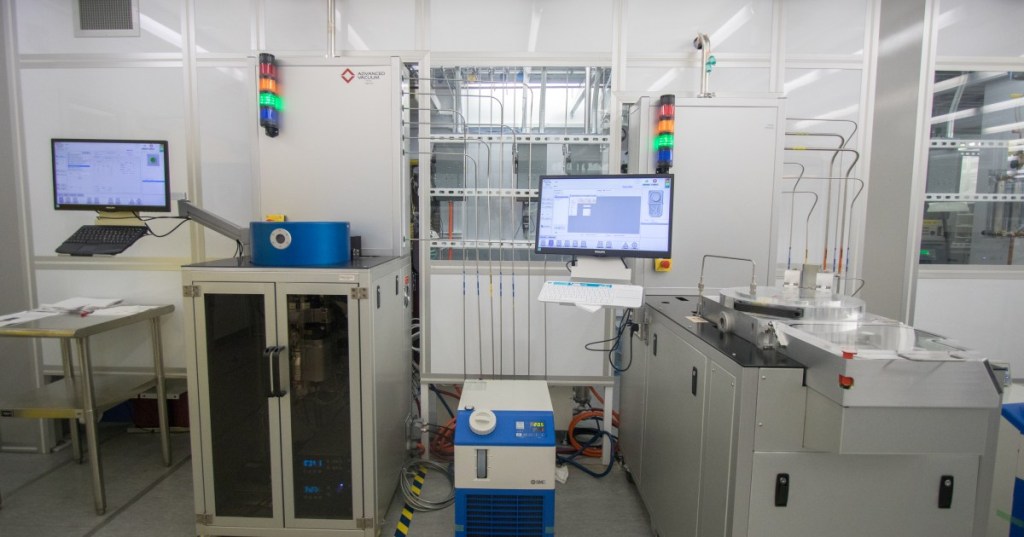
Featured image: UC Davis Center for Nano-MicroManufacturing cleanroom, including dry-etch equipment. Photo by UC Davis College of Engineering / Lucy Knowles, via Wikimedia Commons, CC BY 2.0; cropped to 1200×630 for BitcoinVersus.Tech.
Support and donation options are available through BitcoinVersus.Tech.
BitcoinVersus.tech is not a financial advisor. Content is provided for informational purposes.


Leave a comment