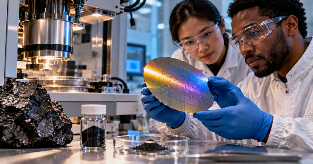
University of Illinois researchers and the U.S. Department of Energy’s National Energy Technology Laboratory have used carbon nanodots made from processed coal to solve a difficult manufacturing problem in two-dimensional transistors: growing an ultrathin insulating layer without damaging the atomically thin semiconductor underneath.
The work uses carbon nanodots about 1 to 5 nanometers wide and one atomic layer thick as an interfacial layer between molybdenum disulfide, or MoS₂, and a high-κ dielectric. Illinois says the result produced dielectric layers with an equivalent oxide thickness of 0.6 nanometers and leakage current density below 0.1 mA/cm².
The Problem Is The Missing Surface Bonds
Silicon is easy to integrate with many familiar chip-fabrication processes because its surface provides chemical bonding sites. Those sites help engineers grow or deposit insulating materials above the transistor channel.
Two-dimensional semiconductors are different. Materials such as MoS₂ can be only a few atoms thick and have surfaces with no dangling bonds. That is useful because it reduces some forms of electron scattering, but it also means common dielectric-deposition processes have very little chemistry to grab onto.

That interface problem has been one of the major obstacles to turning impressive 2D transistor experiments into manufacturable devices. BitcoinVersus.Tech’s semiconductor-device-physics lesson explains why the channel, gate, and dielectric all have to work together for a field-effect transistor to switch cleanly.
The Nanodots Act Like An Atomic Primer Coat
The researchers processed bituminous coal into graphene-like carbon nanodots. Their flat faces attach to the MoS₂ through van der Waals attraction rather than strong chemical bonding, helping preserve the underlying 2D channel.
The edges of the nanodots contain functional groups that can bond with the oxide deposited above them. In effect, one side interacts gently with the 2D semiconductor while the other side provides nucleation sites for the dielectric.
Qing Cao described the layer as a kind of atomic-scale primer coat. That is a useful way to think about it: the carbon dots give the next manufacturing step a surface it can grow on without forcing the transistor channel itself to become chemically rougher.
The Carbon Dots Are Packed Into A Single Layer
The team used a Langmuir-Schaefer assembly process to pack the nanodots tightly together. They dispersed the particles in a solvent, spread the mixture across water, allowed the solvent to evaporate, and mechanically compressed the remaining carbon dots into a dense monolayer.
That monolayer was transferred onto the 2D semiconductor. The researchers could then use atomic layer deposition to grow a smooth high-κ dielectric above it.
Atomic layer deposition is important because it builds material in tightly controlled surface reactions, often one molecular layer at a time. That kind of precision is increasingly important as semiconductor fabrication moves toward angstrom-scale structures, a trend BitcoinVersus.Tech covered in ASM’s push toward atomic-precision chip processing.
The Dielectric Reached A 0.6-Nanometer Equivalent Thickness
The finished dielectric stack reached an equivalent oxide thickness of 0.6 nm. Equivalent oxide thickness compares the electrical behavior of a modern dielectric stack with the thickness of silicon dioxide that would produce similar gate capacitance.
Smaller EOT generally gives the gate stronger electrostatic control over the channel, which becomes increasingly important as transistors shrink. At the same time, the insulator must keep leakage under control. Illinois reports leakage below 0.1 mA/cm², meeting the relevant targets cited from the IEEE International Roadmap for Devices and Systems.
This connects directly with the basic MOSFET behavior covered in BitcoinVersus.Tech’s MOSFET operation lesson: the gate dielectric must electrically couple the gate to the channel while preventing ordinary current from simply leaking through the insulator.
The Researchers Built Working Logic
The team did more than characterize the dielectric. They fabricated field-effect transistors and integrated logic gates using the interface and reported operation around 0.5 volts.
Illinois compares that with roughly 0.6 to 0.8 volts for today’s advanced silicon technologies. Lower operating voltage can reduce switching energy, although a laboratory device still has a long path before it can be compared directly with a production logic process on density, speed, yield, reliability, and cost.
Why MoS₂ Is Attractive Beyond Silicon Scaling
When silicon channels become extremely thin, surfaces and interfaces increasingly affect electron transport. Atomically thin materials such as MoS₂ can maintain a well-defined channel at dimensions where bulk silicon becomes harder to control.
The attraction is not that MoS₂ automatically replaces silicon. The challenge is integrating contacts, dielectrics, interconnects, doping strategies, and wafer-scale manufacturing around the 2D material. Recent working MoS₂ circuits show that the field is progressing beyond isolated transistor records, but fabrication remains the central problem.
That makes this result complementary to other semiconductor scaling work BitcoinVersus.Tech has covered, from plasma etching and photolithography and photoresist to Hyper-NA EUV research. Shrinking features only helps if every material interface can survive the process.
The Strange Part Is Where The Material Came From
Coal is normally associated with bulk energy production, not atomically clean transistor interfaces. The Illinois-NETL team had to spend significant effort purifying the derived carbon material and checking that contaminants incompatible with CMOS fabrication were not present.
The useful property is not “coal” itself. It is the nanoscale carbon structure that can be extracted and processed from it. Once refined, the graphene-like nanodots provide a combination of van der Waals adhesion on one side and oxide-friendly chemistry on the other.
What Comes Next
The next question is whether the process can scale cleanly across large wafers with the uniformity and contamination control required by semiconductor manufacturing. A useful interface on a small research device must eventually work across huge numbers of transistors with extremely tight process variation.
If that happens, carbon nanodots could become one of the small but important process layers that make 2D transistors manufacturable—not because they replace the semiconductor, but because they solve the interface sitting directly on top of it.
Editor’s Note
The featured image is original photorealistic editorial artwork created specifically for this story and is not reused in the body. The body image is a separate University of Illinois photograph of Qing Cao. The YouTube video is embedded as a responsive native Gutenberg player, and the Reddit discussion is embedded directly in the article. No normal story text is placed inside cards, panels, callouts, or text boxes.
BitcoinVersus.Tech content is provided for informational and educational purposes.


Leave a Reply