
Two years after researchers demonstrated a functional graphene semiconductor, the answer to “what replaces silicon?” looks less like a single material and more like a hybrid architecture.
BitcoinVersus.Tech first covered the U.S.-China graphene semiconductor breakthrough in January 2024. Graphene is still in the race. But IBM’s new 7Å NanoStack work, commercial progress in photonic interconnects and rapid advances in other two-dimensional materials now suggest the future chip will combine several technologies rather than crown one universal replacement for silicon.
IBM’s 7Å NanoStack changes the question
IBM Research unveiled its first 0.7 nm, or 7-angstrom, NanoStack technology in June 2026. NanoStack places nanosheet transistors vertically instead of relying only on shrinking them across a flat surface. IBM projects roughly 50% higher performance at the same power or about 70% lower power at the same performance versus its 2 nm reference, while nearly doubling transistor density.
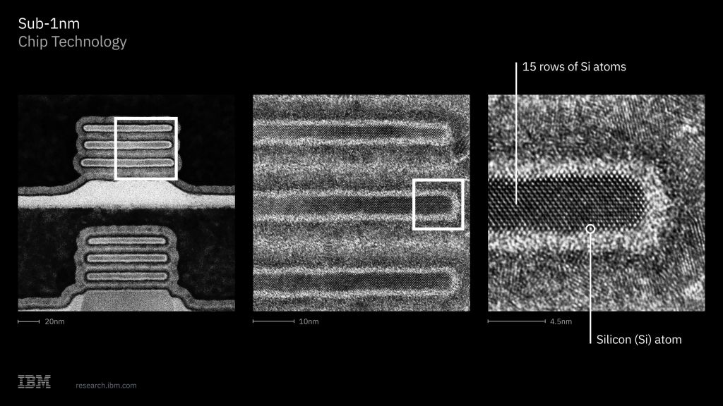
The “7Å” label should not be read as one universal 0.7-nm physical dimension inside the finished chip. Modern process-node names describe a technology generation. More important than the label is the architecture: IBM is moving transistor scaling into the Z axis, and says individual stacked layers can eventually use different channel materials.
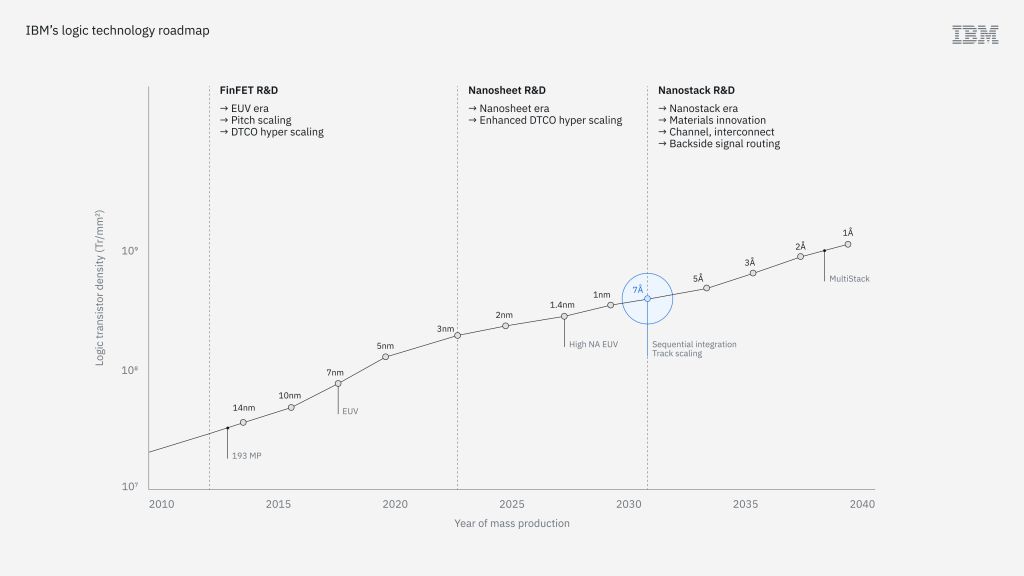
The follow-through is now visible. On October 13, 2026, IBM announced an early research-and-development process design kit for 7Å NanoStack planned for the first quarter of 2027. On October 14, IBM and Siemens announced joint work on the design, simulation, lithography and manufacturing tools needed to push NanoStack toward future production. That does not make 7Å a shipping mass-market node yet, but it moves the architecture from a device demonstration toward an ecosystem that chip designers and manufacturing-tool companies can begin preparing for.
Graphene is still an option
Graphene’s historical weakness was its lack of a useful intrinsic bandgap. The 2024 Georgia Tech-led work changed that discussion by demonstrating semiconducting epigraphene with a 0.6 eV bandgap and room-temperature mobility above 5,000 cm²/V·s. That is why graphene should not be written off simply because silicon has continued scaling.
China Science highlighted the Georgia Tech/Tianjin University graphene-semiconductor result when the Nature paper was published in 2024.
But graphene now looks more likely to become one material inside a heterogeneous device than the sole replacement for silicon CMOS. A 2026 wafer-scale transistor demonstration even used an atomically thin graphene edge as the gate for a vertical MoS₂ device—showing how graphene and another 2D semiconductor can work together instead of competing.
MoS₂ may be the stronger transistor-channel candidate
For the transistor channel itself, molybdenum disulfide and related transition-metal dichalcogenides may currently have the stronger scaling case. A September 2026 Nature Communications study demonstrated monolayer MoS₂ transistors with physical channel lengths below 5 nm, on/off ratios above 10⁶ and a CMOS-compatible process across a 4-inch wafer.
That fits with another trend we have been following in 2D transistor fabrication: silicon does not have to disappear for atomically thin materials to become strategically important. They can be inserted into selected transistor layers where electrostatics or channel thickness become limiting.
Photonics is likely to arrive first around the transistor
Photonics is further along commercially, but mainly as the communication fabric between chips. AI and high-performance computing systems increasingly lose power and performance moving data between processors, memory and switches. That makes optical links an immediate engineering target even while the processors themselves remain electronic.
That is consistent with our recent coverage of Georgia Tech’s silicon-photonic scaling work. Photonics does not need to replace the transistor to become essential. It can replace increasingly expensive electrical links around the compute die first.
The most likely architecture
| Technology | Most likely role | Near-term outlook |
|---|---|---|
| 3D silicon CMOS / NanoStack | Core logic | Highest |
| Silicon photonics / CPO | Chip-to-chip and rack-scale communication | Already entering systems |
| MoS₂ and other 2D semiconductors | Future ultra-thin transistor channels | Strong research trajectory |
| Graphene | Specialized channels, gates, interconnects, RF and heterogeneous layers | Still viable, but unlikely to replace everything |
| Fully photonic logic | Specialized accelerators | Longer-term |
The most probable post-silicon chip is therefore not really “post-silicon.” It is a 3D heterogeneous semiconductor: vertically stacked CMOS logic, specialized 2D-material layers where they outperform silicon, advanced memory and packaging, and optical links carrying data between dense compute blocks.
IBM’s NanoStack strengthens that forecast because it makes material diversity part of the architecture itself. Graphene remains relevant. Photonics may become unavoidable. MoS₂ may win some future transistor layers. But the architecture most likely to dominate is the one that combines them.
BitcoinVersus.Tech Editor’s Note:
We volunteer daily to ensure the credibility of the information on this platform is Verifiably True. If you would like to support to help further secure the integrity of our research initiatives, please donate using the QR code provided

For best QR-code scanning results, please scan this donation code from a desktop or larger screen. Mobile screens may prevent camera recognition.


Leave a Reply