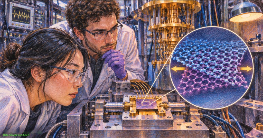
University of Washington physicists have demonstrated a powerful new way to tune electrical transport in magic-angle twisted bilayer graphene: stretching its atomic lattice. Their peer-reviewed Science paper, published November 12, 2026, reports an elastoresistance gauge factor more than two orders of magnitude larger than in conventional metals. The measurement reveals extreme sensitivity to mechanical deformation; it does not demonstrate a commercial processor or a 100-fold reduction in electricity use.
Graphene is a single-atom-thick sheet of carbon. Stack two sheets and rotate them by approximately 1.1 degrees, and the overlapping atomic lattices produce a larger repeating moiré pattern. Near the so-called magic angle, electron interactions can support insulating and superconducting states under carefully controlled laboratory conditions. Earlier post-silicon computing research examines why such material properties interest chip engineers even before a practical device exists.
Matthew Yankowitz of the University of Washington discusses ‘Giant elastoresistance in magic-angle twisted bilayer graphene’ in a January 15, 2026 National MagLab seminar. Original technical presentation predating the November publication; credit: National MagLab / YouTube.
A controlled stretch changes an atomic-scale lattice
The new experiment adds a mechanical control variable to the better-known controls of twist angle, temperature, carrier density and electric field. Researchers working with Matthew Yankowitz and Jiun-Haw Chu mounted microscopic graphene structures on an actuator that expands or contracts under applied voltage. The device lets the team vary uniaxial strain continuously instead of treating accidental lattice distortion as a fabrication error.
Elastoresistance describes the change in electrical resistance caused by strain. A gauge factor compares a fractional resistance change with the applied deformation. The reported result means graphene’s strain response exceeded a conventional metal’s response by more than 100 times in the experimental conditions. It does not mean the device’s total resistance became 100 times smaller, nor that its circuit efficiency improved by the same amount.
What the 100-fold comparison measures
The effect depended on how electrons filled available states and on temperature. In selected carrier-density regimes, the scientists observed a strong increase in the response as temperature fell, with behavior resembling a Curie–Weiss relationship. The paper discusses several possible microscopic origins, including electronic nematic fluctuations and fluctuating spin- or valley-like degrees of freedom. Those explanations remain subjects for investigation rather than settled diagnoses.
Precise control over correlated electronic states is a research capability, not a universal on/off switch. The original magic-angle superconductivity result required temperatures near absolute zero, and the UW result does not establish ambient-temperature superconductivity. The recent work on ultra-thin multiferroic films offers another experimental path toward electrical control of magnetic behavior, but the underlying physics is different.
Pablo Jarillo-Herrero presents the 2018 original magic-angle graphene superconductor results at an American Physical Society meeting. Historical context, not footage of the University of Washington’s 2026 strain experiment. Credit: American Physical Society / YouTube.
The distance between a lab effect and a working chip
The distinction also matters for energy claims. A measurable resistance response does not, by itself, specify how much energy a logic gate would consume, how much an actuator costs to operate, or whether billions of devices can be fabricated consistently. Scaling atomic-layer assembly, maintaining the twist angle, integrating strain controls and operating at practical temperatures all remain difficult engineering problems.
Researchers hope their approach can help compare superconductors, insulators and other correlated phases using a single adjustable sample. The method may eventually inform new sensors or quantum-material experiments. It has no published manufacturing roadmap or demonstrated performance advantage over standard silicon transistors. Readers can compare the electrical-contact challenges of semiconductor devices and the wider graphene, diamond and photonics outlook before treating an elegant physics experiment as a near-term chip forecast.
The practical advance is a repeatable new tuning technique. By making strain a controllable laboratory parameter, the UW researchers can probe electronic behavior that was previously difficult to separate from uncontrolled deformation. Independent replication across materials and temperatures will determine how broadly the technique applies.
Primary references: University of Washington news release, November 12, 2026; Xuetao Ma and colleagues, “Giant elastoresistance in magic-angle twisted bilayer graphene,” Science, November 12, 2026, DOI: 10.1126/science.adz0597; independent edited republication of the UW release, November 12. The report distinguishes the peer-reviewed measurement from proposed applications.
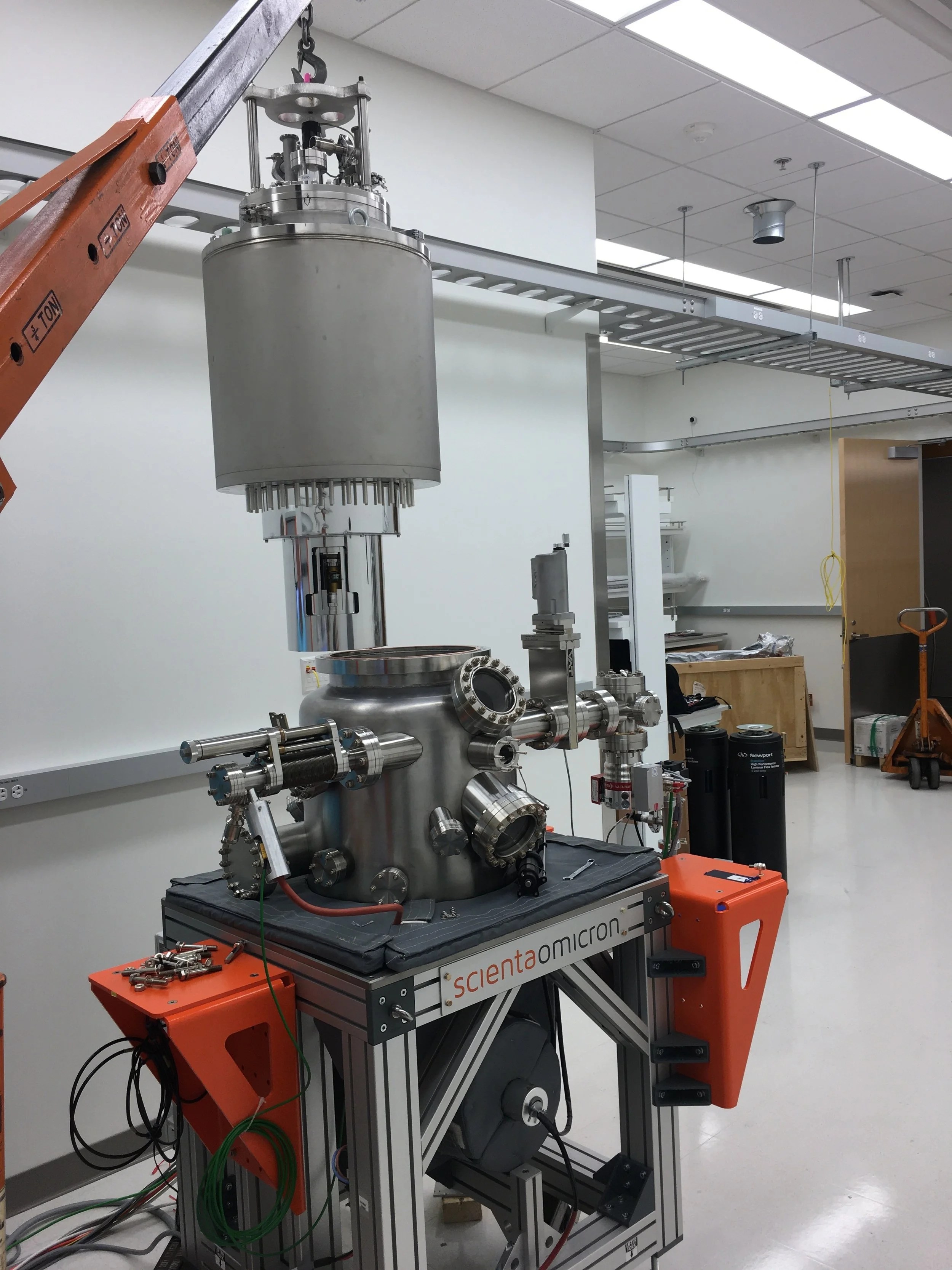
Editor’s Note: The result concerns mechanical strain sensitivity in a cryogenic correlated-electron system, not verified processor energy savings, high-temperature superconductivity, or commercial-scale production. The original colored-pencil 1200 × 630 featured cover is conceptual artwork with fictional researchers, a stylized graphene lattice and a neon-green Bitcoinversus.tech watermark. The in-story equipment photo is authentically sourced from the research lab and provides general context rather than documenting the specific experiment. Two original-source YouTube talks explain the new and historical physics; WordPress iframe rendering alone cannot prove mobile playback.

BitcoinVersus.Tech is volunteer-run and publishes independent technical journalism. An optional 5,000-satoshi donation supports ongoing research. Scan the original QR from a second screen using a compatible Bitcoin wallet; on the same phone, use a wallet that can import a saved QR image when supported. Independently verify recipient 3C9o19EH5HSiwEPyCTmEKzxhNCbo2X6TTb and the 5,000-satoshi amount before sending. Bitcoin transfers are generally irreversible.
We volunteer daily to ensure the information on BitcoinVersus.Tech is Verifiably True. Technical and financial coverage is educational and informational, not personalized engineering, securities, tax or investment advice.


Leave a Reply