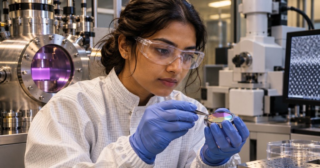
November 2, 2026 — Brown University researchers in Providence, Rhode Island, have reported a way to retain both electric and magnetic order in ultrathin bismuth ferrite, even at just four atomic unit cells, approximately 1.6 nanometers. Their October 28 study in Nature Materials advances a potential building block for low-power logic and memory, rather than demonstrating a finished processor.
The obstacle has been the “dead layer”: as multiferroic films shrink, disrupted crystal structure and unwanted electric fields can erase the properties engineers hope to exploit. In its research announcement, Brown explains how the team tackled both mechanisms instead of simply making a thicker film.
Engineering Away the Dead Layer
The researchers grew bismuth ferrite on a dysprosium scandate substrate, using lattice mismatch to compress and stabilize the film. A conductive strontium ruthenate layer screens disruptive electric fields. The combined boundary conditions preserved ferroelectric and magnetic behavior at device-relevant thicknesses, according to atomic-resolution imaging, magnetic measurements and calculations.
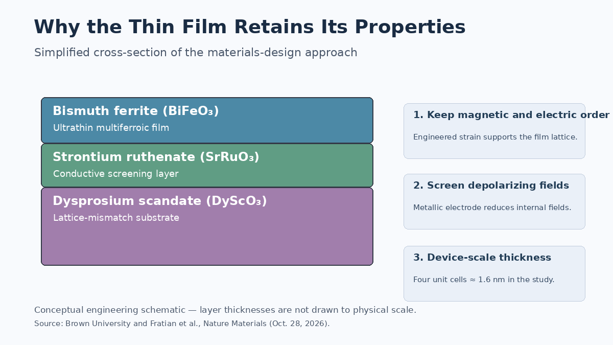
Importantly, the experiments also showed signatures of altermagnetism, a magnetic ordering pattern of interest because it may support dense, fast information readout. This is a materials result: the paper does not report a working AI chip, a processor clock rate, or a verified reduction in energy per computation.
What the Thickness Data Really Show
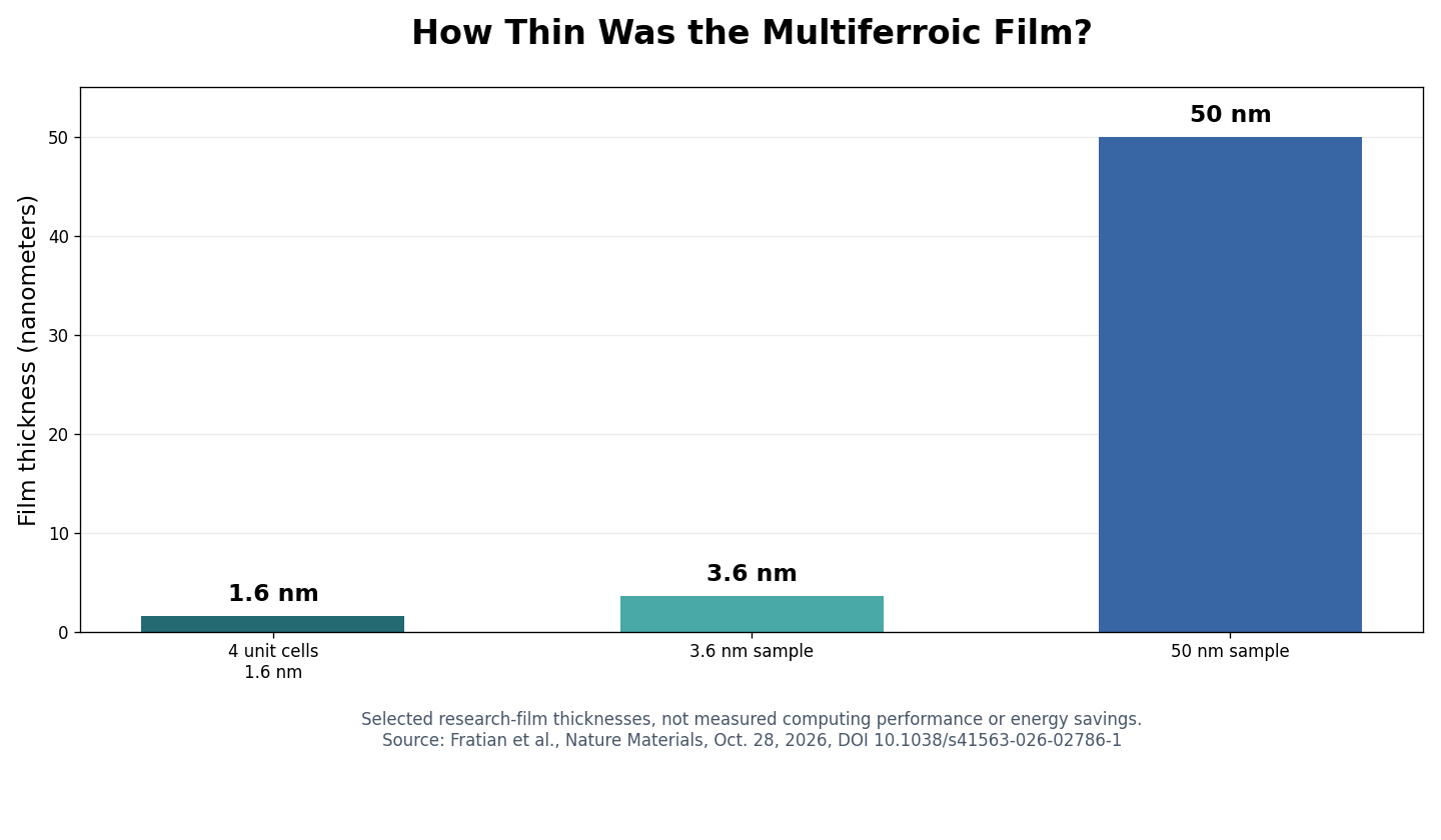
The study examines film thicknesses including 1.6, 3.6 and 50 nanometers. Those numbers describe research samples, not a performance comparison. We use a vertical bar chart rather than a time-series line because these are discrete thickness groups, not measurements changing over time.
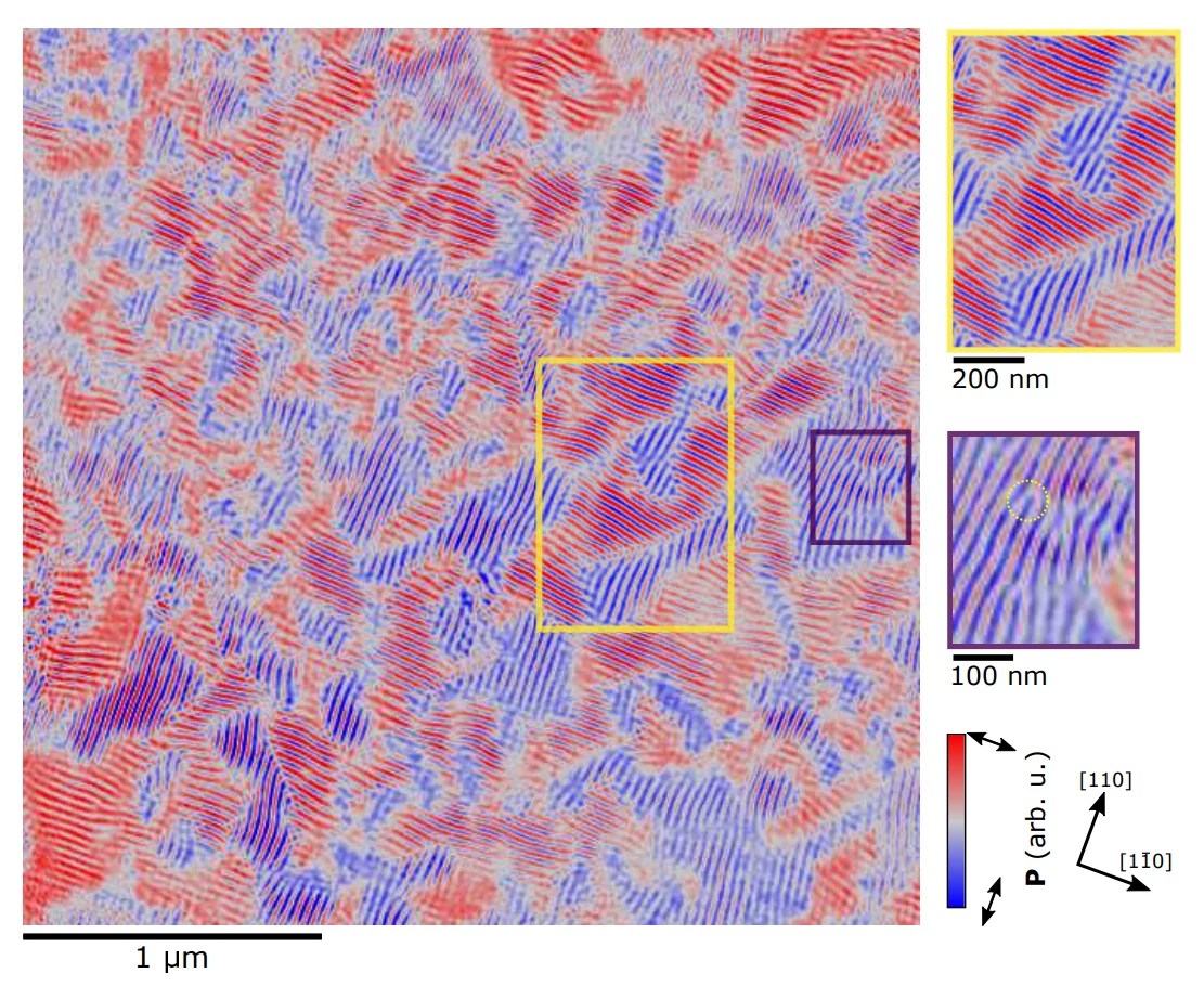
Earlier 2024 work at Switzerland’s Paul Scherrer Institute imaged coupled magnetic and ferroelectric textures in bismuth ferrite. Its picture below illustrates the established physical phenomenon; it is not an image from Brown’s new experiment.
Why It Matters—and What Is Missing
For computing, the attraction is nonvolatile switching driven by modest voltage pulses. But progress in post-silicon chip materials and gallium-nitride power devices shows that promising laboratory physics and scalable manufacturing remain separate challenges.
The practical comparison is with devices already shipping or being commercialized. Our reports on ultralow-power microcontrollers, semiconductor process contamination and edge-AI silicon track different pieces of that transition.
Next come device prototypes, repeatable switching and endurance tests, compatibility with semiconductor fabrication, and measured energy-per-operation results. Until those data exist, claims of dramatically more efficient AI chips remain prospects, not demonstrated system-level savings.
BitcoinVersus.Tech
BitcoinVersus.Tech Editor’s Note: We volunteer daily to ensure the credibility of the information on this platform is Verifiably True. If you would like to support our work and help further secure the integrity of our research initiatives, please scan the QR code below to donate 5,000 sats. For best results, scan the QR code from a laptop or larger screen.

Bitcoin donation address: 3C9o19EH5HSiwEPyCTmEKzxhNCbo2X6TTb. On mobile, open the QR on another screen or use your wallet’s saved-image scanner.
Disclaimer: BitcoinVersus.Tech reports technology, energy and financial developments for informational purposes only, not investment advice. Experimental materials results and projected future computing benefits are subject to further scientific and engineering validation.


Leave a Reply