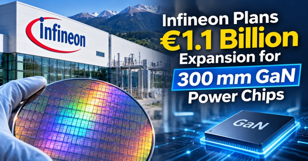
Infineon Technologies announced October 27 that it will invest approximately €1.1 billion in its Villach, Austria, semiconductor facility through 2034 to establish high-volume manufacturing of gallium nitride power chips on 300-millimeter wafers. The project is intended to serve growing demand for efficient power conversion in AI data centers, electric vehicles and industrial equipment, with production scheduled to begin by the end of 2027.
The European Commission approved €319 million in Austrian state aid for the expansion under the European Chips Act. The separate formal funding commitment from Austria remains pending, Infineon said.
Why 300 mm Wafers Matter
Gallium nitride, or GaN, is a wide-bandgap semiconductor used in power switches that control the flow and conversion of electricity. Compared with conventional silicon-based devices, properly designed GaN circuits can switch at higher frequencies and reduce losses, enabling smaller power supplies and less waste heat.
The manufacturing shift is equally significant. Infineon says a 300 mm wafer can yield approximately 2.3 times as many chips as a 200 mm wafer. That is a wafer-level comparison, not proof that every finished chip will cost less: usable yield, processing complexity and factory utilization still determine the economics.
Infineon demonstrated processing of 300 mm GaN wafers in 2024. Its new investment aims to translate that milestone into industrial-scale manufacturing using existing and upgraded cleanroom infrastructure in Villach.
Power Chips for AI Infrastructure
Power semiconductors are distinct from the GPUs that train AI models. They sit in the electrical systems that transform and regulate energy before it reaches servers, storage and networking hardware. Improving conversion efficiency can reduce electricity losses and cooling requirements, although actual savings depend on the complete system design.
The expansion also has industrial-policy implications. The European Commission describes the facility as first-of-a-kind in the European Union and expects the project to support collaboration with universities, research organizations and smaller semiconductor companies.
Infineon’s plan does not mean 300 mm GaN chips are already shipping at volume. The announced timetable calls for production to begin by late 2027, followed by a market-dependent ramp. The next milestones are formal Austrian funding, equipment installation, production qualification and evidence of commercial yields.
Related: Enphase and Infineon Test 900 V GaN Switch for AI Data-Center Power, which covers device-level technology rather than this manufacturing expansion.
Editor’s Note: We volunteer daily to ensure the credibility of the information on this platform is Verifiably True. If you value this reporting, consider donating 5,000 sats using our Bitcoin donation QR code; for best results, scan it from a laptop or larger screen using your phone’s Bitcoin wallet.
Bitcoin donation address: 3C9o19EH5HSiwEPyCTmEKzxhNCbo2X6TTb
To scan the QR code below, open this page on another screen and scan it with your mobile Bitcoin wallet. If your wallet supports scanning a saved image, you can save the QR image and scan it from your phone instead.

BitcoinVersus.tech is not a financial advisor. This media platform reports on financial subjects purely for informational purposes.


Leave a Reply