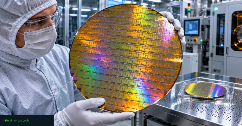
Silicon carbide (SiC) is a wide-bandgap semiconductor used in power electronics to switch high voltages and currents with comparatively low losses. Infineon Technologies announced on November 9, 2026, that it had fabricated functional power devices on 300-millimeter SiC wafers at its Villach, Austria, factory, using existing silicon-manufacturing equipment. Infineon describes the demonstration as an industry first in a full-scale fabrication environment. The milestone establishes process feasibility, not the start of commercial high-volume SiC production.
Infineon Technologies, “Inside the 300mm Fab for Thin Silicon Wafers,” July 25, 2019. Official archival film of silicon-wafer manufacturing at Villach; it does not show November 2026 silicon-carbide processing.
Why wafer diameter matters
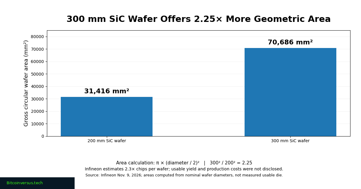
A semiconductor wafer is a circular substrate processed into many individual chips. Moving from 200 mm to 300 mm increases the nominal area according to the square of the diameter: (300 ÷ 200)² = 2.25. The ideal circular area therefore rises from approximately 31,416 mm² to 70,686 mm², an increase of 125%. Infineon separately estimates 2.3 times as many chips per wafer, allowing for its design and manufacturing assumptions. Neither figure represents a disclosed count of good commercial chips.
Greater wafer area can improve output per processing cycle, but usable dies depend on defect density, edge losses, device size, substrate cost and yield. A working wafer is an important engineering demonstration; volume economics require repeatability across many wafers. Related production constraints appear in BitcoinVersus.Tech’s coverage of Bosch’s SiC manufacturing qualification and Wolfspeed’s silicon-carbide capacity plans.
A second breakthrough in wafer splitting
Infineon also reported demonstrating its Cold Split process on 300 mm SiC at Dresden, Germany. The technique aims to separate thin wafers from a SiC crystal boule with less lost material and shorter processing time than traditional wire sawing. The company has not disclosed a validated commercial manufacturing cost per wafer or a date for scaling the new 300 mm SiC process.
Infineon Technologies, “Infineon’s Groundbreaking 300 mm Power GaN Technology,” September 11, 2024. Official demonstration of a different wide-bandgap material—gallium nitride—not the newly reported SiC wafer.
SiC, GaN and the power demand ahead
SiC switches are increasingly used in electric-vehicle traction inverters, charging systems, industrial drives, renewable-energy converters and high-voltage data-center equipment. Infineon’s existing 800 VDC power collaboration and Vertiv supply agreement illustrate demand for more efficient power conversion. Better switching devices can reduce specific electrical losses, but savings depend on the complete system design.
The November announcement must also be separated from Infineon’s €1.1 billion plan, unveiled October 27, for high-volume 300 mm gallium-nitride manufacturing at Villach. That distinct project targets production by the end of 2027. Infineon has not assigned the same date to 300 mm silicon carbide. The differences between the materials and roadmaps matter for assessing Infineon’s earlier GaN expansion and its newer SiC work.
Infineon plans to exhibit the processed SiC wafer at electronica in Munich beginning November 10. The next tests are commercial: wafer quality, repeatable device performance, supply of suitable substrates and economically viable yields. Potential benefits do not yet establish a cost reduction or a completed production transition.
Primary sources: Infineon, November 9, 2026, 300 mm SiC announcement; Infineon–Wolfspeed 200 mm SiC supply agreement, October 15; Infineon 300 mm GaN expansion, October 27.
BitcoinVersus.Tech Editor’s Note
Reviewed November 9, 2026. The functional-device milestone, 2.3× estimated chips per wafer and Cold Split feasibility are company-reported results. The 2.25× geometric-area comparison is calculated from nominal diameters; no production yield or cost saving was independently demonstrated. The featured image is conceptual artwork, not a photograph of Infineon’s actual SiC wafer. Both official videos predate the announcement and depict different wafer technologies.
We volunteer daily to ensure the information on this platform is Verifiably True. If you would like to support the research, please scan QR code.

Support independent research with an optional donation of 5,000 satoshis. Scan the original QR with a Bitcoin wallet on another screen, or use a compatible saved-image scanner on mobile. Verify destination 3C9o19EH5HSiwEPyCTmEKzxhNCbo2X6TTb and amount before sending.
BitcoinVersus.Tech is not a financial advisor. Financial coverage is provided purely for informational purposes.


Leave a Reply