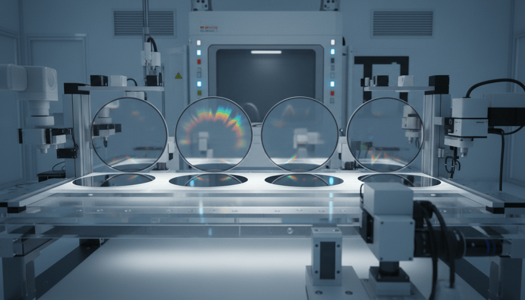
Global silicon wafer shipments reached 3,756 million square inches in the third quarter of 2026, up 13.4% from 3,313 million square inches a year earlier, according to figures released November 4 by semiconductor industry association SEMI. Volume also rose 5.1% from the preceding quarter’s 3,573 million square inches. The measurements describe substrate area shipped by wafer suppliers, not finished chip output, semiconductor revenue or the number of operating fabrication plants.
The rebound offers a materials-level view of demand extending beyond the most advanced processors. SEMI attributed stronger shipments to artificial intelligence, recovering industrial demand, power devices, photonics and advanced packaging. The industry group did not provide a breakdown proving how many square inches were destined for each application.
Why wafer area matters
A silicon wafer is a carefully prepared crystalline disk onto which semiconductor manufacturers build circuits through deposition, lithography, etching and other steps. Wafer makers generally report shipments by area because customers purchase multiple diameters and grades. A square inch of polished silicon does not translate into a fixed number of chips: die size, usable yield, process complexity and wafer diameter all influence output.
SEMI’s comparison implies an increase of 443 million square inches from the year-earlier quarter. The sequential gain was 183 million square inches. Those are observed shipment differences, not projected additions to fab capacity. The figures also should not be interpreted as evidence that every chipmaker is growing at the same rate.
Recent Siltronic wafer-demand reporting provides a company-level view of the materials market, while BitcoinVersus.Tech’s global fab-capacity forecast concerns planned manufacturing infrastructure rather than current substrate shipments.

AI demand spreads into supporting chips
Masatsugu Miura, chairman of SEMI’s Silicon Manufacturers Group and a SUMCO executive, said AI-related demand had expanded from advanced logic and memory into power devices and photonics. Industrial applications, including robotics and server power supplies, also contributed to improving conditions. His comments describe an industry assessment, not a published customer-by-customer sales ledger.
Power semiconductors regulate and convert electricity delivered to computing equipment. Photonic devices help move data over optical links. Advanced packaging connects multiple dies and memory components in high-bandwidth assemblies. Growing demand for any of those functions can support additional wafer consumption without implying that every new wafer becomes an AI accelerator.
For context, Tower and Innolight’s optical-chip production update illustrates one application area. Infineon’s planned 300 mm gallium-nitride expansion shows another, although GaN-on-silicon manufacturing and conventional silicon wafer statistics should not be treated as identical product categories.
A recovery indicator, not a production guarantee
Higher wafer shipments can precede more semiconductor fabrication, but inventories, customer ordering patterns and fabrication yields complicate any direct conversion into finished-device production. The quarterly statistics also cannot establish utilization rates, profit margins or whether demand will persist into 2027.
The next test is whether material orders remain firm as new fabrication capacity, advanced packaging lines and AI infrastructure move from announced projects to actual operation. For now, SEMI’s reported 13.4% annual increase is a measurable improvement in the upstream supply chain, with important limits on what the number alone can prove.
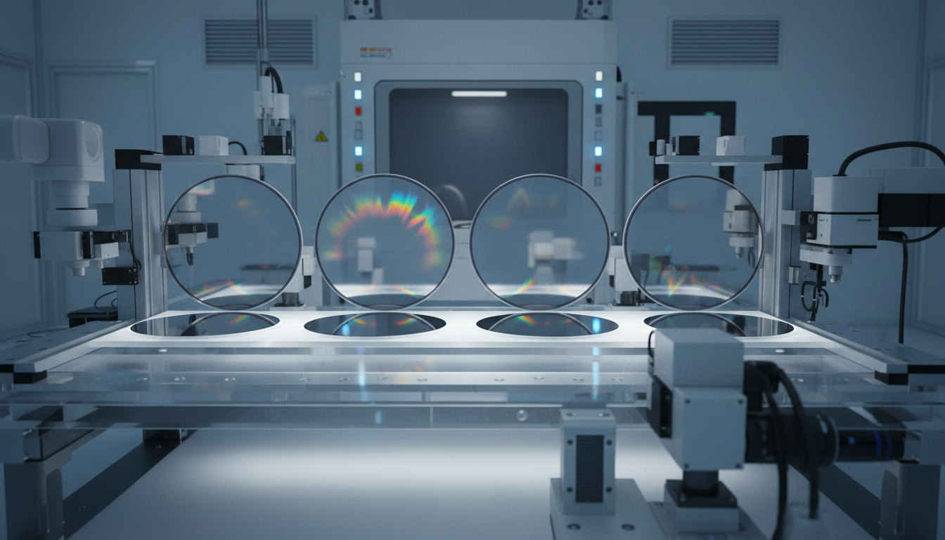
Editor’s Note: Shipment totals and percentage changes were checked against SEMI’s November 4, 2026 announcement. Figures describe silicon wafer area shipped, not chips manufactured or installed fab capacity. The wafer illustration is AI-generated and does not depict a documented manufacturing facility. No independent audit of SEMI’s underlying survey responses was conducted.

To donate 5,000 satoshis, display the original Bitcoin donation QR on a second screen and scan it with a compatible Bitcoin wallet. On mobile, use another device or a wallet’s supported saved-image QR scanning function. Confirm the displayed payment destination before transferring funds.
We volunteer daily to ensure the information on this platform is Verifiably True. If you would like to support the research, please scan QR code.


Leave a Reply