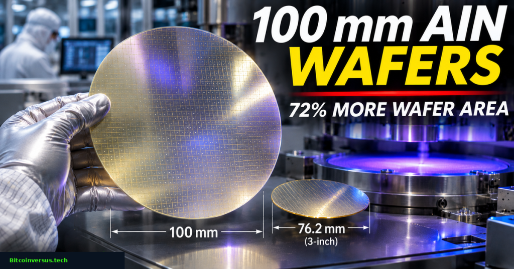
HexaTech has begun offering 100-millimeter single-crystal aluminum nitride (AlN) substrates, a larger wafer for ultraviolet emitters, radio-frequency components and next-generation power electronics. The November 3, 2026 announcement follows the company’s February launch of a three-inch, or 76.2 mm, AlN wafer. The new diameter provides 72.2% more gross surface area per circular wafer, although neither chip yield nor device output can be inferred from diameter alone.
AlN is a direct-bandgap semiconductor with an energy gap near 6.1 electronvolts. Its electrical insulation, heat conduction and compatibility with aluminum-rich gallium-nitride device layers make it attractive for high-power switching and deep-UV optoelectronics. Scaling crystal size is necessary for economic fabrication: bigger substrates can accommodate more device patterns and fit additional industrial equipment.
DARPAtv’s February 2023 educational session on wide- and ultra-wide-bandgap semiconductor devices. Background materials science, not video of HexaTech’s November 2026 product. Source: DARPA/YouTube.
The mathematics behind 72% more area
For a circular wafer, surface area equals π multiplied by the square of half its diameter. A 76.2 mm wafer contains about 4,560 square millimeters of gross area; a 100 mm wafer contains 7,854 square millimeters. Dividing 7,854 by 4,560 gives approximately 1.722, or a 72.2% increase. Compared with a two-inch (50.8 mm) wafer, the 100 mm wafer has 3.88 times as much geometric area.
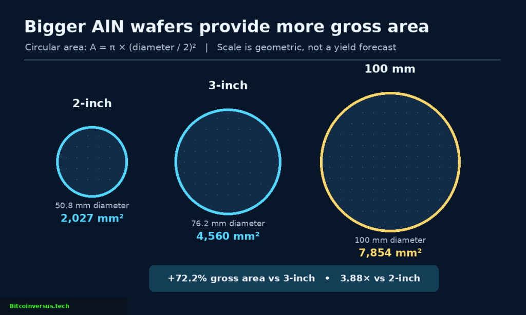
Real device yield depends on usable edge area, crystalline dislocations, film quality, lithography, test results and how circuits tile the surface. Larger diameter does not guarantee 72% more saleable devices. The distinction matters as global wafer shipments increase and factories evaluate competing substrate technologies.
Growing crystals above 2,000 degrees Celsius
HexaTech produces single-crystal boules by physical vapor transport, or PVT: a hot AlN source releases vapor species that condense onto a cooler seeded growth region. Its published process description places crystal growth above 2,000°C. Finished boules are sliced, polished and characterized before manufacturers deposit functional semiconductor layers.
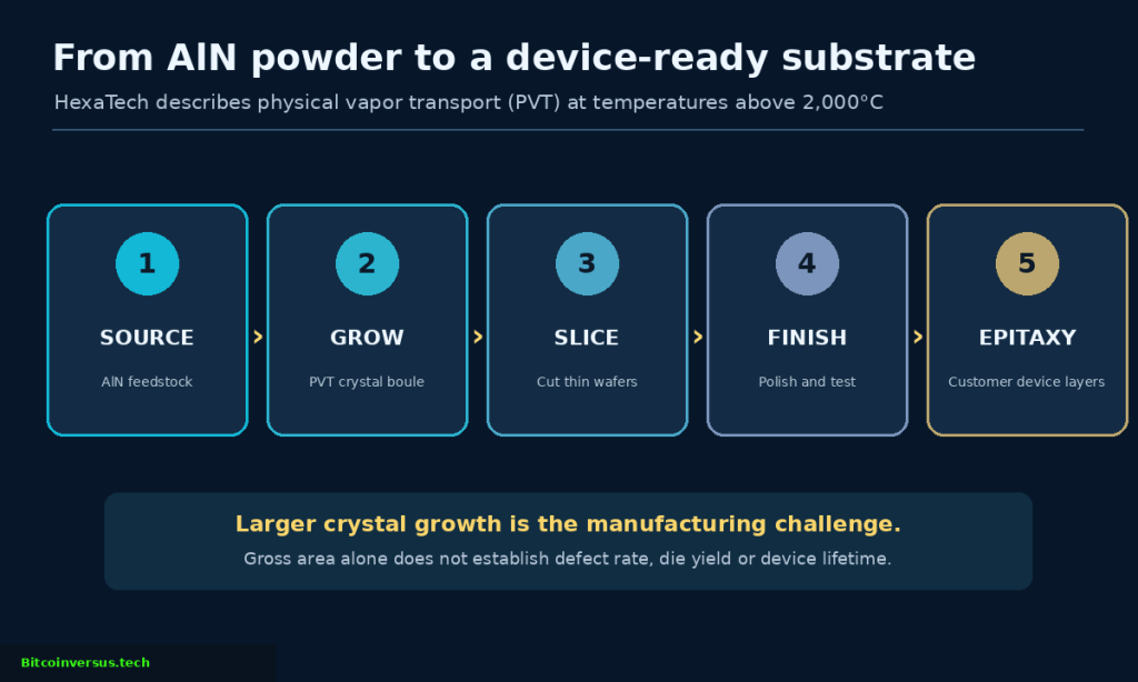
The engineering challenge extends beyond diameter. Large crystals must preserve acceptable structural quality across the full disc and survive wafer finishing, handling and device processing. Suppliers also need repeatable thickness, bow, surface preparation and production economics. Similar integration challenges appear in lithography equipment upgrades and the transition to larger packaging formats.
HexaTech is not the first to reach 100 mm
Asahi Kasei reported that its subsidiary Crystal IS produced a 100 mm single-crystal AlN substrate in 2023. In June 2024, the company said its serial-production substrates had reached 99% usable area against specified UV-C LED requirements. Those are competitor-reported results, not published yield figures for HexaTech. HexaTech’s November milestone is commercial release of its own 100 mm product, rather than a world-first diameter record.
DARPA’s December 2018 historical panel on earlier wide-bandgap GaN programs. The video gives semiconductor-development context; it does not demonstrate HexaTech’s AlN wafer or establish its performance. Source: DARPA/YouTube.
HexaTech says two-inch, three-inch and 100 mm products are available with standard lead times. Its roadmap points toward 150 mm and beyond, but the announcement supplies no volume shipped, wafer pricing, defect-density map for the larger size or confirmed commercial device yields. A previous DARPA program supported research toward low-defect 100 mm AlN, while other fabrication developments, including high-voltage AI power electronics, show possible end markets rather than guaranteed customers.
The immediate progress is measurable: more available substrate area from an additional supplier. Whether the larger wafers lower cost per functioning UV-C emitter or high-voltage device depends on production quality and adoption, not the diameter calculation alone.
Editor’s Note
Sources: HexaTech’s November 3 and February 10, 2026 releases, published growth-process documentation, and Asahi Kasei’s 2023–24 Crystal IS announcements. The 72.2% and 3.88× figures are geometric calculations, not measured chip yields or selling-price reductions. Both DARPA YouTube videos are older educational background, not footage of HexaTech’s announcement. The featured cover is a conceptual illustration rather than an authenticated factory photograph. Video identity and rendered players are checked separately from actual playback and embedding permission.
Support BitcoinVersus.Tech
An optional 5,000-satoshi donation supports volunteer research. Scan the original QR with a compatible Bitcoin wallet. When reading on one phone, open the code on another screen or use the wallet’s supported saved-image scanner. Verify the destination and amount before sending.

We volunteer daily to ensure the information on this platform is Verifiably True. If you would like to support the research, please scan QR code.


Leave a Reply