
A modern AI accelerator is more than a single silicon die. Leading designs connect processor chiplets, high-bandwidth memory stacks and specialized interconnects inside one package. Advanced packaging shortens electrical paths and helps move data across components, but assembly capacity can become a bottleneck even when chip fabrication plants have already produced the silicon.
Investment is following that constraint. In a November 6 Reuters report, semiconductor research firm Yole Group forecast advanced-packaging capital spending approaching $28 billion in 2026. Yole also expects advanced-packaging revenue to exceed traditional-packaging revenue for the first time during the year. Both are industry forecasts, not audited full-year results.
Applied Materials’ official animated explainer, “The World of Advanced Packaging,” published April 16, 2021, illustrates how logic chiplets and stacked memory are assembled. Background technology footage, not an announcement of 2026 spending. Credit: Applied Materials/YouTube.
Why chip assembly became a production constraint
TSMC’s CoWoS packaging platform integrates compute chips and high-bandwidth memory through a common interposer and substrate. The CoWoS-S, CoWoS-R and CoWoS-L variants offer different interconnect technologies and package sizes. TSMC says CoWoS entered volume production in 2012; later generations expanded package complexity as AI demand accelerated.
The added assembly step helps explain why a company can secure leading-edge wafers yet face limits on finished accelerator shipments. BitcoinVersus.Tech previously compared NVIDIA and AMD accelerator specifications; memory bandwidth and power figures depend partly on technologies assembled inside the finished package, not merely transistor-node dimensions.
Why equipment suppliers are targeting square panels
Conventional packaging frequently uses circular 300-millimeter wafers. Applied Materials describes development of larger rectangular panel substrates and says its equipment can process panels as large as 600 by 600 millimeters. The intended advantage is space for more or larger package structures per processing run, with reduced geometric waste from fitting rectangular units onto a circular wafer.
A 300-mm circular wafer has a gross area of approximately 70,686 square millimeters. A 600 × 600-mm square panel has 360,000 square millimeters. Dividing the latter by the former gives a 5.09× geometric-area ratio, before subtracting edge exclusions or unusable regions.
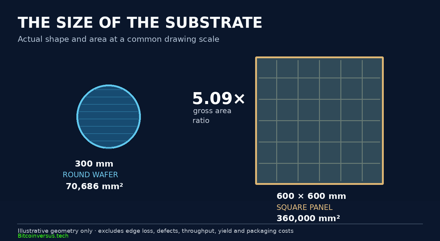
Crucially, greater panel area does not demonstrate 5.09 times more good devices or proportionately cheaper packages. Yield, substrate warpage, fine-line lithography, equipment utilization, defect inspection and bonding accuracy still determine productive output. Applied Materials’ Topaz panel-deposition tools establish an equipment capability, not proof that every AI accelerator uses a 600-mm panel.
The race includes new tools and untested economics
In May, Applied Materials announced a proposed acquisition of NEXX, describing the business as an expansion of its panel-packaging deposition portfolio. BitcoinVersus.Tech previously covered Applied Materials and Besi’s hybrid-bonding work, an adjacent manufacturing challenge, and Hummink’s micron-scale repair module, which addresses defects rather than panel size.
The supply picture is broader than a single manufacturer. Recent growth in silicon wafer shipments concerns upstream material volume, whereas advanced-packaging spending concerns downstream assembly infrastructure. Expanding one stage without the other can shift a bottleneck rather than eliminate it.
The next useful benchmarks are qualified monthly packaging capacity, yield after assembly, cost per good accelerator, memory-interconnect reliability and the delivery of committed tools. Capital-spending forecasts and commercial throughput should remain separate until comparable production figures are available.
Sources and methodology
Reuters (November 6, 2026, reporting Yole Group’s industry forecast); TSMC CoWoS platform specifications; Applied Materials advanced-substrate documentation; Topaz PVD product description; Applied Materials NEXX announcement (May 3, 2026). The underlying Yole research model was not independently accessible for audit.
Editor’s Note: The $28 billion figure is a 2026 capital-spending forecast attributed to Yole Group through Reuters, not audited expenditure. The 5.09× ratio compares gross substrate geometry only and excludes defect rates, usable area and process economics. The featured colored-pencil cover is a conceptual illustration of semiconductor packaging, not a documented TSMC or Applied Materials production line. The Applied Materials video is archival technical context, not evidence of 2026 spending or verified playback.
Support BitcoinVersus.Tech
For an optional 5,000-satoshi contribution, scan the original BitcoinVersus.Tech donation QR below using a compatible Bitcoin wallet. On a phone, display the article on another screen or use a wallet’s supported saved-image scanning feature. Confirm the destination and amount before approving payment.

We volunteer daily to ensure the information on this platform is Verifiably True. If you would like to support the research, please scan QR code.


Leave a Reply