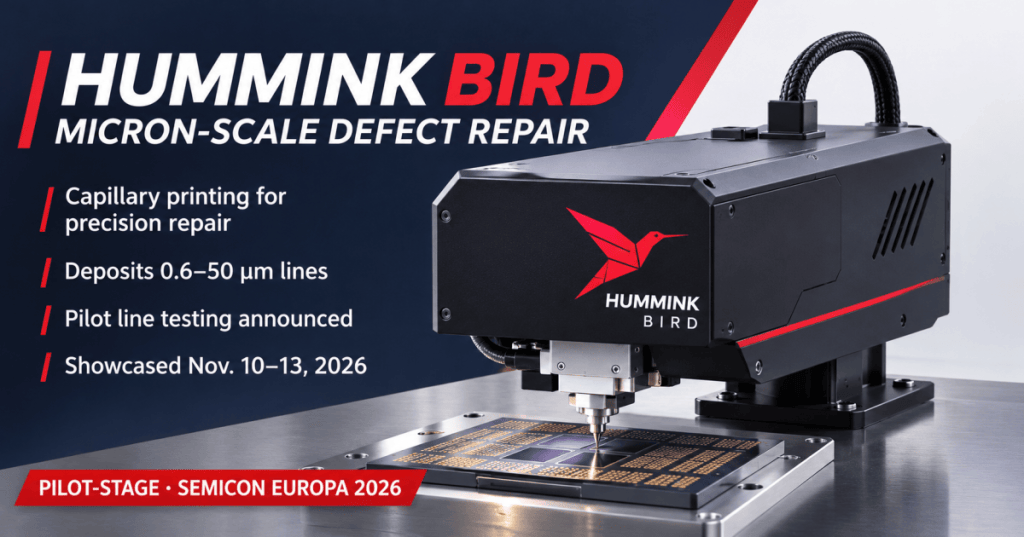
French microprinting developer Hummink plans to showcase its BIRD module at SEMICON Europa in Munich from November 10–13, 2026. The system targets microscopic defects in semiconductor packaging and display manufacturing through localized material deposition. Hummink says the module has entered a pilot line at an unnamed semiconductor and display manufacturer in Asia, but has not disclosed verified commercial yield improvements, customer identity or full-scale production figures.
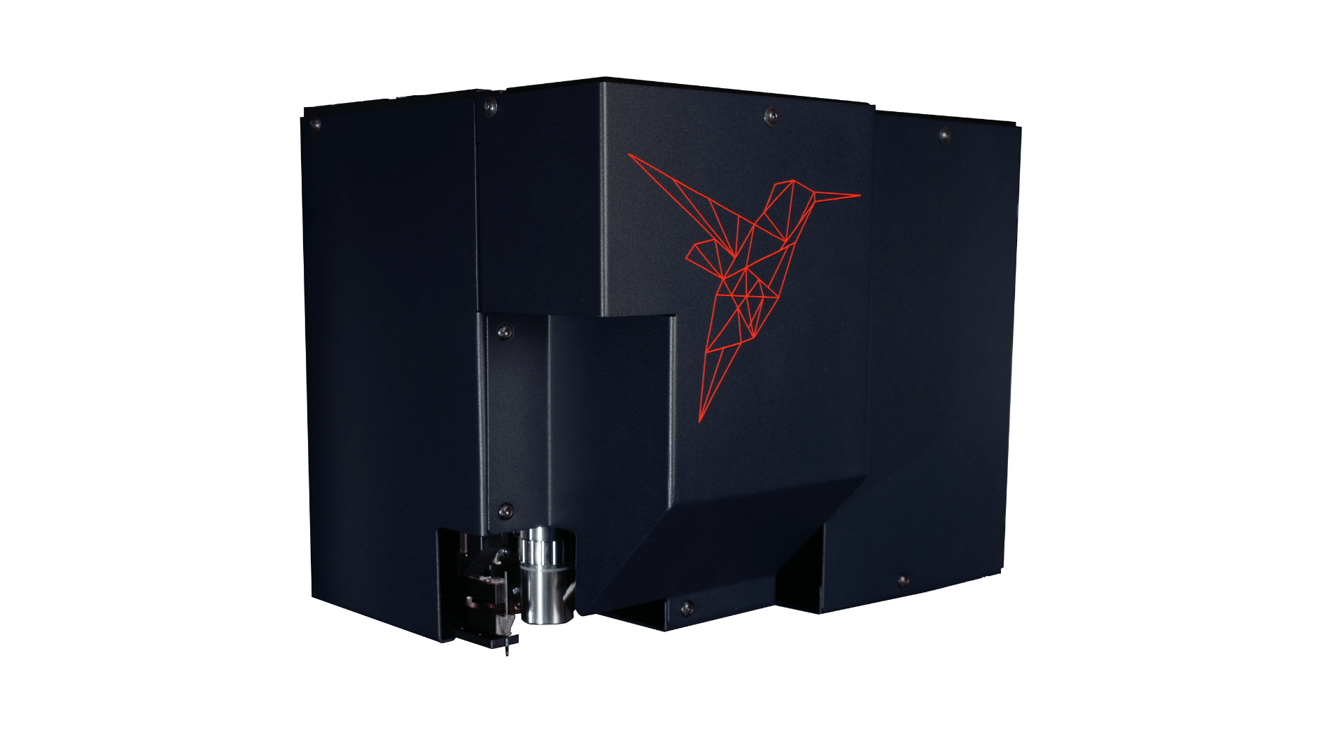
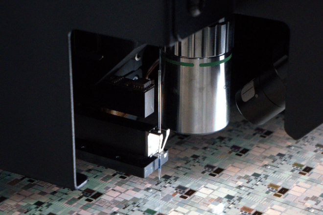
BIRD stands for Breakthrough Integration and Resolution in Defect Repair. Its underlying process, High Precision Capillary Printing (HPCaP), uses a fine pipette and capillary forces to dispense ink precisely where additional material is needed. Unlike broad-area coatings or conventional lithography, the additive approach can concentrate a repair on a damaged conductor or other small feature without patterning an entire substrate.
Why tiny defects threaten expensive chip packages
Advanced packages connect multiple silicon dies through fine redistribution layers (RDLs) and interposers. An electrical open or missing line may spoil a high-value assembly even when most components are functional. BitcoinVersus.Tech has explained 2D and 3D packaging architecture and previously covered new silicon-interposer manufacturing. Both developments place greater importance on inspecting and controlling dense interconnects.
Hummink advertises BIRD printing features from 0.6 to 50 micrometers and support for conductive, dielectric and other functional inks at viscosities up to 250,000 centipoise. The company also lists compatibility with glass and multiple substrate materials. It describes a maskless process followed by localized laser sintering, which consolidates deposited material. The manufacturer presents a workflow lasting minutes, although no standardized throughput comparison or independent yield study was provided.
Pilot installation does not establish volume production
Hummink’s October announcement calls the Asian deployment a pilot. The SEMICON Europa exhibitor listing independently confirms the planned booth and product description, but reproduces vendor-supplied specifications rather than reporting factory inspection results. Buyers still need evidence of repeatability, contamination control, repair resistance, defect-detection integration and throughput under actual line conditions.
The European Commission’s BIRD project report describes work on integrating the technology into production tools and cites research on printed silver structures. It documents technical development, not certification that every micro-scale packaging defect is repairable. Older Hummink NAZCA laboratory printers also have different operating specifications; measurements for those research systems should not be substituted for BIRD’s industrial claims.
The manufacturing case depends on measurable yield
Repairing an otherwise unusable panel could save materials and preserve valuable chips. Yet additional inspection, ink handling, sintering, process qualification and equipment maintenance all carry cost. Incomplete repairs or material incompatibility can still force rejection. BitcoinVersus.Tech’s guide to semiconductor metrology and inspection explains why defect detection and measurement must accompany corrective processes.
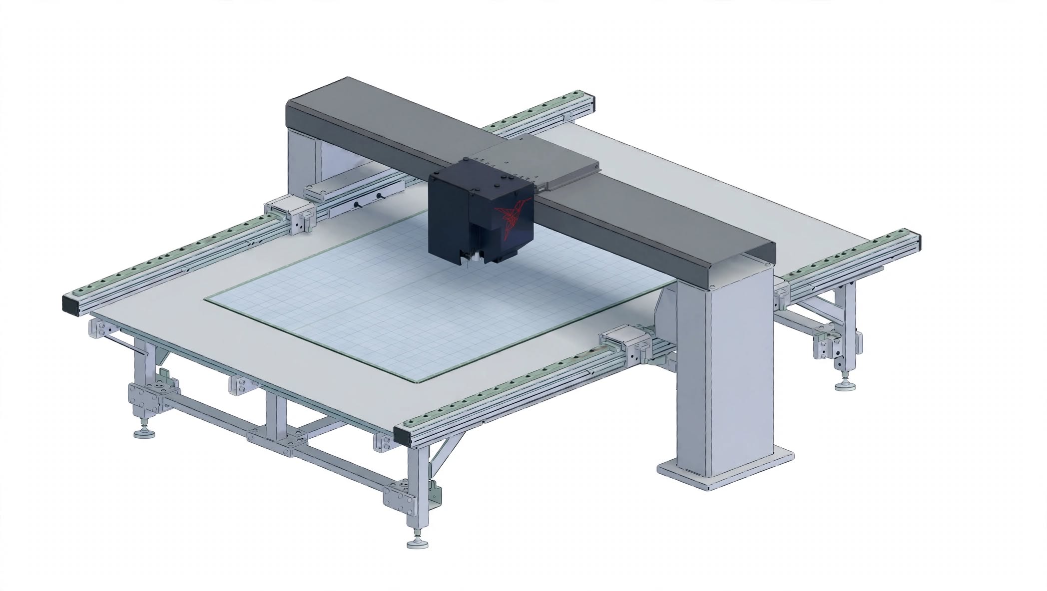
For chip manufacturers, the practical test will be documented repair yield, electrical reliability and cycle time per acceptable part. The planned Munich introduction marks another step toward industrial qualification, not a proven high-volume semiconductor repair rollout. Earlier BitcoinVersus.Tech coverage of lithography process windows offers additional context for how narrow manufacturing margins make defect control essential.
Editor’s Note: BIRD technical claims, the 0.6–50 µm range, the 250,000 cP ink rating and the Asia pilot statement were checked against Hummink’s October 2026 announcement and the SEMI exhibitor listing. Development context was checked against the European Commission’s BIRD project reporting. The company has not published independently confirmed production-scale semiconductor yield data. Images are official product material; the featured cover is an editorial illustration. Hummink’s 2024 YouTube video is historical background. Live player playback and independent mobile/desktop visual inspection remain unverified.

To donate 5,000 sats, open the article on a separate display and scan the original QR code with a compatible Bitcoin wallet. On mobile, use another screen or your wallet’s supported image-scanning feature. Verify the destination 3C9o19EH5HSiwEPyCTmEKzxhNCbo2X6TTb before sending.
We volunteer daily to ensure the information on this platform is Verifiably True. If you would like to support the research, please scan QR code.


Leave a Reply