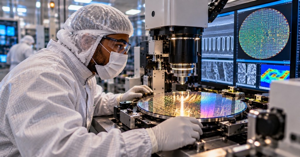
Semiconductor metrology answers “how much?” while inspection answers “what is wrong and where?” Both are process-control tools. Metrology measures quantities such as critical dimension, film thickness, overlay, wafer shape, and topography. Inspection searches for particles, pattern defects, scratches, edge damage, and other abnormalities that can reduce yield.
This lesson follows OSSTC.007: Wafer Probe Testing. Probe testing asks whether devices electrically work. Metrology and inspection help determine whether fabrication stayed within physical targets before final electrical test.
Hitachi High-Tech demonstrates a modern CD-SEM platform used for semiconductor critical-dimension measurement.
Learning Objectives
- Distinguish metrology from defect inspection.
- Explain film thickness, critical dimension, overlay, topography, and wafer geometry.
- Describe optical inspection, ellipsometry, CD-SEM, and defect review.
- Read wafer maps and recognize spatial defect signatures.
- Explain why calibration, reference standards, recipes, and sampling plans matter.
- Troubleshoot common measurement and inspection problems.
Metrology and Inspection Are Different Jobs
KLA describes semiconductor metrology systems as tools used to measure pattern dimensions, film thickness, film stress, layer-to-layer alignment, pattern placement, surface topography, and electro-optical properties. Its inspection systems identify, locate, characterize, review, and analyze defects on patterned and unpatterned wafers.
A thickness tool may report that a dielectric film is above target. An inspection tool may instead report a cluster of particles near one wafer edge. One is a numerical process shift; the other is a spatial defect pattern.
Wafer Maps Are Diagnostic Tools
Measurement and inspection results are often displayed as wafer maps. Spatial information matters because center, edge, radial, repeating, or localized patterns can point toward hardware or process causes.
- Edge ring: may suggest edge handling, bevel contamination, edge-exclusion behavior, or chamber geometry.
- Center-to-edge gradient: may suggest process nonuniformity, temperature variation, flow distribution, plasma distribution, or optical-model error.
- Localized cluster: may suggest particle generation, chuck contamination, robot contact, a damaged carrier, or a tool hotspot.
- Repeating die pattern: may point toward lithography, reticle, design-sensitive, or systematic effects.
- Random distribution: may indicate broad contamination or a stochastic defect mechanism.
A recent metrology discussion focuses on how wafer measurement data is analyzed across multiple tools and why mapping matters.
Optical Wafer Inspection
Optical inspection illuminates the wafer and analyzes reflected or scattered light to detect defects quickly across large areas. Bright-field and dark-field methods emphasize different defect types and surface responses. Modern systems combine advanced illumination, sensors, stage control, design information, and classification algorithms.
Optical inspection usually provides much higher wafer throughput than electron-beam review, so fabs often use optical tools to find candidate defects and slower review tools to characterize selected defects in greater detail.
Film Thickness and Ellipsometry
Spectroscopic ellipsometry measures how polarized light changes after interacting with the wafer. Software fits the optical response to a material model to estimate thickness and related optical constants.
The result depends on both the instrument and the model. A stable optical path is not enough if the recipe assumes the wrong layer stack, refractive-index model, angle, wavelength range, or material structure.
Covalent demonstrates spectroscopic ellipsometry mapping of silicon-on-insulator wafers and shows how uniformity can be measured non-destructively.
Critical Dimension and CD-SEM
Critical dimension, or CD, is a measured width or feature size that must stay within process limits. NIST identifies critical-dimension and overlay metrology as core semiconductor-fabrication measurements and notes that CD-SEM is a major industry technique because electron-beam imaging provides high spatial resolution.
A CD-SEM scans a focused electron beam across the structure and forms an image from emitted electron signals. Charging, contamination, beam conditions, focus, astigmatism, pattern contrast, recipe placement, and image-processing settings can all influence the reported result.
Overlay Metrology
Overlay measures how accurately one patterned layer is aligned to another. NIST describes overlay as a critical quality-control measurement because layer-to-layer misalignment can make devices nonfunctional even when each individual layer is correctly patterned.
Wafer Geometry and Surface Topography
Wafer geometry tools measure properties such as thickness, flatness, bow, warp, nanotopography, and edge roll-off. These influence lithography focus, bonding, handling, polishing, and downstream process uniformity.
Optical profilometers and interferometric methods can measure step height and three-dimensional surface topography. In advanced packaging, similar metrology is used for bump height, redistribution-layer dimensions, TSV structures, bonded wafer shape, and other 3D features.
A recent semiconductor discussion highlights the challenges created by surface topography, advanced materials, 3D structures, tool integration, cleanliness, and production requirements.
Defect Review Comes After Detection
An inspection tool may flag thousands of candidate locations. Review tools inspect selected defects at higher resolution to determine what they actually are. Preserve coordinates, wafer orientation, defect ID, recipe, tool ID, lot information, and process history so the review remains traceable to the original event.
Calibration, Reference Standards, and Matching
Metrology depends on traceable, stable measurement. Precision is not the same as accuracy. A tool can repeatedly return nearly the same number and still be biased. Calibration standards, reference wafers, tool-to-tool matching, preventive maintenance, and statistical monitoring are part of the measurement system.
- Precision: repeated measurements agree closely.
- Accuracy: the measurement is close to the accepted or traceable value.
- Repeatability: the same tool under the same conditions reproduces the result.
- Reproducibility: results remain comparable across operators, tools, sites, or changing conditions.
- Tool matching: multiple production tools measure the same reference material closely enough for the process-control requirement.
Sampling and Statistical Process Control
Not every wafer and every die can always receive every expensive measurement, so fabs use sampling plans. Those plans specify which lots, wafers, die, sites, and process steps are sampled. Technicians should not casually change sample sites or recipes to make a run finish because the new location may not be statistically equivalent to the established control location.
Troubleshooting Order
- Confirm wafer ID, lot ID, orientation, and recipe.
- Check whether the failure affects one wafer, one lot, one tool, or multiple tools.
- Verify reference-wafer or calibration performance before blaming the process.
- Inspect the chuck, stage, handling path, optics, vacuum system, and contamination-sensitive surfaces appropriate to the tool.
- Check recipe targeting, alignment, focus, pattern recognition, and measurement-site coordinates.
- Compare raw images or signals with prior known-good runs instead of relying only on the final number.
- Review wafer-map shape for center, edge, radial, repeating, or localized signatures.
- Check tool alarms, chamber pressure, beam current, source condition, sensor condition, and environmental stability as applicable.
- Compare against a matched tool or certified reference when available.
- Escalate to process engineering after the measurement system itself has been reasonably cleared.
Hands-On Exercise
Create a mock wafer map with 49 measurement sites. Give the center sites a film thickness of 100.0 nm and gradually increase the edge sites to 104.0 nm. Calculate the center average, edge average, wafer average, range, and percent nonuniformity using the method defined by your lab or class.
Then create three defect maps: one random, one edge-ring, and one localized cluster. For each map, write three possible equipment or process causes and list the measurements you would take before changing the process tool.
Knowledge Check
- What is the difference between metrology and inspection?
- Why is a wafer map more useful than only a wafer-average number?
- What does a CD-SEM measure?
- What does overlay metrology evaluate?
- Why can ellipsometry report a wrong result even when the instrument is stable?
- What is the difference between precision and accuracy?
- Why verify a reference wafer before declaring a process excursion?
- Why can moving a measurement site change the apparent process result?
Answers
- Metrology measures a physical quantity; inspection searches for and locates defects or abnormalities.
- The spatial pattern can reveal center-edge, radial, localized, repeating, or handling-related signatures that an average hides.
- Critical dimensions and related nanoscale pattern dimensions using scanning-electron imaging and measurement algorithms.
- How accurately one patterned layer aligns to another.
- The optical model or layer-stack recipe can be wrong even if the hardware is stable.
- Precision is agreement among repeated measurements; accuracy is closeness to the accepted or traceable value.
- It helps prove whether the measurement system itself is stable before the process is changed.
- Different wafer locations can have real process gradients, so a new site may not be equivalent to the established control site.
Previous Related Lessons
- OSSTC.007: Wafer Probe Testing
- OSSTC.006: Semiconductor RF Power Delivery
- OSSTC.003: Semiconductor Vacuum Systems
- OSSTC.002: Wafer Handling and FOUPs
- OSSTC.001: Fab Cleanroom, Contamination, and ESD Basics
Primary references: NIST — Critical Dimension and Overlay Metrology, NIST — Overlay Metrology Using Physics and AI-Based SEM, KLA — Defect Inspection and Review, and Hitachi High-Tech — CD-SEM and Defect Inspection.
BitcoinVersus.Tech Editor’s Note:
We volunteer daily to ensure the credibility of the information on this platform is Verifiably True. If you would like to support to help further secure the integrity of our research initiatives, please donate using the QR code provided

BitcoinVersus.Tech provides technical education and analysis for informational purposes only.


Leave a Reply