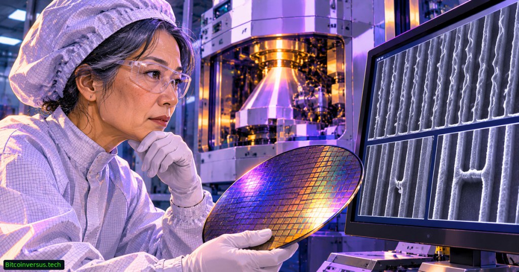
OSSEC.016 examines stochastic defects in extreme-ultraviolet lithography: random printing failures that remain even when average focus, dose and critical dimensions appear acceptable. EUV uses 13.5 nm light to print intricate semiconductor features, but individual photon arrivals and resist chemistry vary locally. Rare line bridges, broken lines and missing contact holes can affect electrical yield. The prior OSSEC.015 explored focus–exposure process windows; the next question is whether apparently acceptable conditions suppress rare failures.
ASML, “Inside the machine: How a High NA system generates EUV light,” August 21, 2025. Official explanation of the 13.5 nm light source and exposure equipment. A lithography-system demonstration, not footage of measured stochastic defects. Credit: ASML / YouTube.
Why a nominally identical pattern can fail
The 2026 imec metrology review distinguishes statistical line roughness from localized catastrophic printing defects. Photon shot noise becomes significant because relatively few high-energy EUV photons contribute to a tiny feature. Chemical composition, electron migration, resist development and mask imperfections introduce additional variability. More dose can reduce one source of noise, but reduces scanner throughput and cannot eliminate all material-related variation.
Line-edge roughness (LER) measures edge-position variation; line-width roughness (LWR) concerns feature width. A bridge joining neighboring printed regions or a broken resist line is a different, discrete failure. Its eventual electrical consequence depends on tone, pattern transfer and device geometry. OSSEC.014 on overlay addresses alignment between layers, not randomness within an individual printed layer.
Inspect large areas without missing nanometer defects
Imec reports stochastic defects of roughly 10 nm and smaller, presenting an inspection tradeoff. Optical inspection can survey large wafer areas quickly but has limited sensitivity to the smallest faults; electron-beam inspection resolves finer structures at lower throughput. Unbiased CD-SEM analysis aims to subtract instrument noise when measuring roughness. Neither a handful of attractive micrographs nor a three-sigma LER statistic alone establishes a failure-free process window.
Hitachi Electron Microscope, “Stochastic defect analysis of EUV lithography photoresist pattern,” December 7, 2020. Original FIB-SEM serial-section demonstration with 1 nm section intervals and a three-dimensional reconstruction of connected resist lines. Credit: Hitachi / YouTube.
In 2021 research on 28 nm-pitch line/space patterns, imec correlated optical and e-beam inspection with electrical test structures. The evidence helps link resist-level bridges or breaks to opens and shorts after pattern transfer. OSSEC.012 on yield explains why defect frequency matters beyond a visually sharp image.
Control the tradeoffs, not only the average
Engineers compare defect counts across comparable wafer regions, exposure settings, resist materials and measurement recipes. Dose, illumination, bake, development and etch conditions can shift failures differently. OSSEC.013 on statistical process control provides drift-monitoring context, while OSSTC.008 introduces inspection tools. A clean SEM frame never proves zero defects across a full wafer.
Engineering conclusion: Successful EUV patterning requires both average dimensional control and adequate sampling for rare stochastic failures. Higher exposure dose, better resists and complementary inspection can help, but each option carries cost, speed or sensitivity limitations.
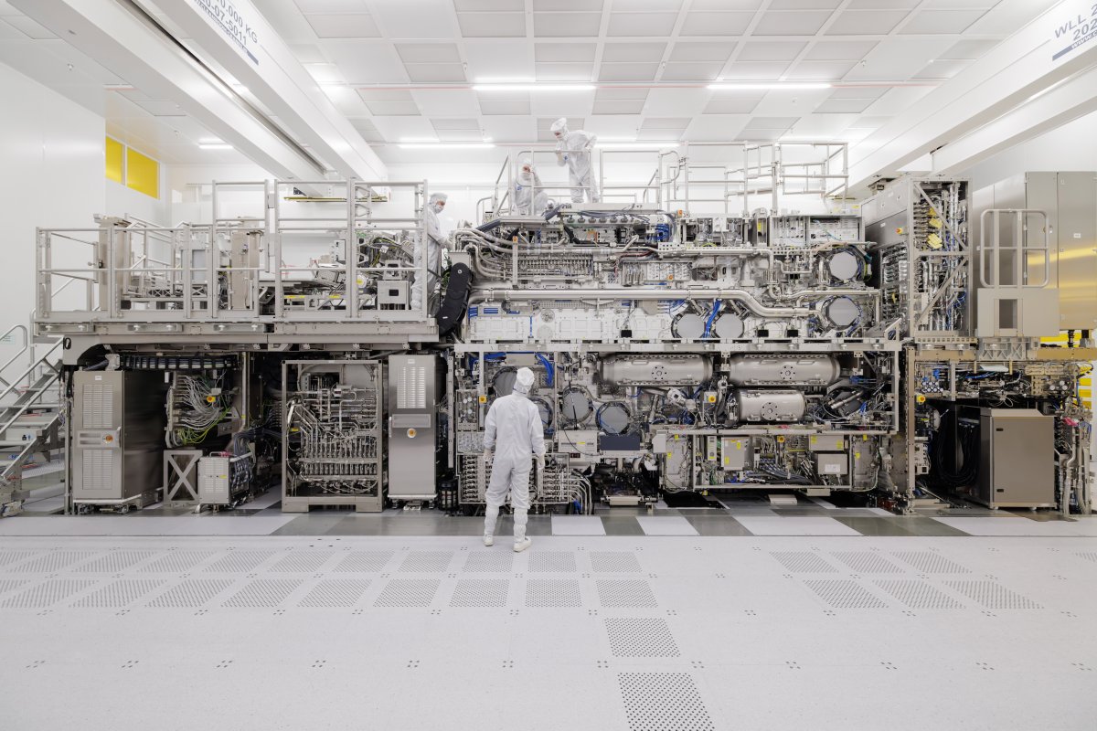
Editor’s Note: Scientific claims were checked against imec research, the ASML EUV specifications and Hitachi’s original microscopy demonstration. The 1200 × 630 anime-style cover is original editorial artwork with a small neon-green Bitcoinversus.tech watermark; the microscopy features visible on the cover are fictional. The article includes a real ASML photograph credited ©ASML and no generated diagrams. No wafer experiment or actual video playback test was performed.

BitcoinVersus.Tech is volunteer-run and publishes independent technology education. An optional 5,000-satoshi contribution supports continued research. Display the original QR on a second screen and scan with a compatible Bitcoin wallet; on the same phone, use a wallet supporting image import. Independently verify recipient 3C9o19EH5HSiwEPyCTmEKzxhNCbo2X6TTb and amount before transferring. Bitcoin payments are generally irreversible.
We volunteer daily to ensure the information on BitcoinVersus.Tech is Verifiably True. Educational coverage does not authorize changes to production semiconductor equipment and does not constitute certified engineering, financial or investment advice.


Leave a Reply