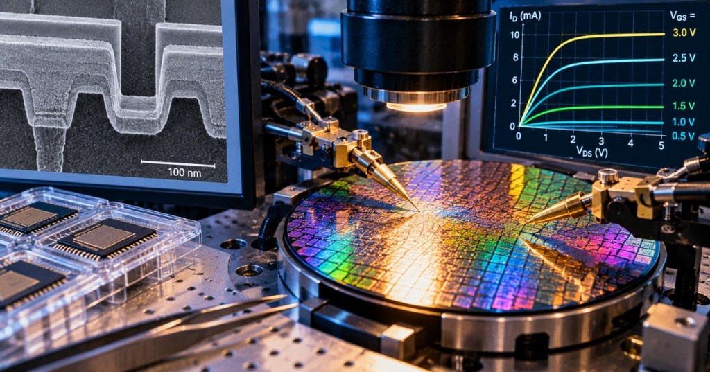
Wafer probe testing is the electrical checkpoint between fabrication and packaging. A probe station or wafer prober positions a wafer, aligns electrical probes to tiny bond pads or test structures, and connects the device under test to instruments that measure current, voltage, capacitance, timing, RF behavior, or full functional performance.
This lesson follows OSSTC.006: Semiconductor RF Power Delivery, OSSTC.005: Semiconductor Pneumatic Systems, and OSSTC.003: Semiconductor Vacuum Systems. The focus now shifts from process equipment to semiconductor test equipment and the technician skills needed to keep measurements repeatable.
Learning Objectives
- Explain what a probe station and wafer prober do.
- Identify the chuck, stage, microscope, manipulators, probes, and probe cards.
- Describe how electrical contact is made to wafer pads.
- Distinguish parametric tests from functional tests.
- Understand how IV and CV measurements fit into wafer characterization.
- Recognize the role of wafer maps and pass/fail binning.
- Troubleshoot contact resistance, alignment, contamination, open circuits, and unstable measurements.
What a Probe Station Does
A probe station is the precision mechanical platform that holds a wafer or die and positions electrical, RF, optical, or other probes over the device. The probe station itself is not the source-measure instrument. It creates a controlled physical interface between the device under test and external equipment such as source-measure units, parameter analyzers, oscilloscopes, network analyzers, or automated test systems.
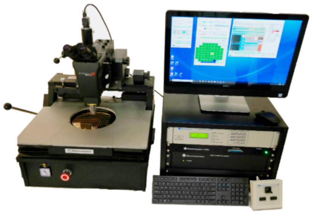
Manual systems rely heavily on an operator for alignment and probe placement. Semi-automatic and fully automatic systems add motorized wafer motion, alignment routines, wafer maps, automated stepping from die to die, temperature control, and software-controlled test sequences.
The Chuck and Stage Hold and Move the Wafer
The wafer normally rests on a very flat chuck. Vacuum is commonly used to keep it from moving. The stage provides X and Y motion to move between devices, Z motion to raise or lower the wafer relative to the probes, and theta rotation to align wafer streets and pads with the probe geometry.
Some chucks also provide heating or cooling so devices can be characterized across temperature. Temperature stability matters because semiconductor leakage, threshold voltage, mobility, resistance, and timing can all change with temperature.
Microscopes and Vision Systems Control Alignment
Electrical pads on semiconductor devices can be extremely small. A microscope or machine-vision system helps align the wafer and probes so the probe tips land on the correct metal pads without contacting nearby structures.
Automatic probers may use wafer-edge detection, alignment marks, pattern recognition, and stored coordinate maps. A small alignment error can create an open circuit, short adjacent pads, damage a pad, or create inconsistent contact resistance across the wafer.
Probe Needles and Probe Cards Make Contact
A manual or characterization station can use individual probes mounted on micropositioners. Production wafer test more often uses a probe card that holds many probe elements in a fixed geometry so multiple pads, and sometimes multiple dies, can be contacted at once.
Probe technologies include traditional cantilever needles, vertical probes, and MEMS-based probe structures. The correct design depends on pad pitch, device current, signal speed, RF requirements, contact force, expected touchdown count, and wafer-level parallelism.
Touchdown Is a Mechanical and Electrical Event
When a probe lands on a metal pad, contact must be strong enough to produce a stable electrical connection but controlled enough to avoid damaging the pad. Many probe tips intentionally scrub or wipe a small distance across the metal surface during touchdown. That movement helps break through native oxide, contamination, or surface films that can otherwise produce high or unstable contact resistance.
Too little overtravel can create intermittent contact. Too much can damage pads, deform probe tips, increase debris, or shorten probe-card life. Technicians should use the qualified contact procedure for the specific probe technology instead of adjusting force or overtravel by feel.
Parametric Tests Measure Device Behavior
Parametric testing measures electrical characteristics rather than only asking whether a completed circuit works. Typical measurements include leakage current, breakdown behavior, threshold voltage, resistance, capacitance, diode characteristics, transistor IV curves, and test-structure measurements used for process control.
An IV measurement changes voltage and measures current, or changes current and measures voltage. A CV measurement changes bias and measures capacitance. Those measurements can reveal device structure, oxide behavior, junction characteristics, doping-related effects, defects, and process variation depending on the test structure.
Functional Wafer Test Screens Complete Dies
Functional wafer test checks whether a die performs its intended operation before packaging. Memory devices may be tested for read/write behavior and bad cells. Logic devices can be exercised with digital patterns. Analog and mixed-signal devices may be tested for gain, timing, offsets, linearity, or conversion accuracy.
Screening defective die before packaging saves downstream cost because expensive assembly, advanced packaging, burn-in, and final test do not need to be performed on obviously failing silicon.
Wafer Maps Turn Test Data Into Spatial Information
Automated test systems typically associate each die with coordinates and a result bin. A wafer map can show pass/fail information and different failure categories across the wafer. Spatial patterns often matter as much as the total yield number.
- Edge-heavy failures may point toward edge-process or handling issues.
- A localized cluster can suggest contamination, equipment nonuniformity, or a reticle-related problem.
- Repeated row or column patterns may indicate stepping, contact, or test-system problems.
- Random isolated failures may indicate device defects, marginal design behavior, or unstable probe contact.
Technicians should avoid assuming that every failing pattern is caused by the wafer. Probe contamination, bent probes, chuck debris, alignment error, tester channels, cables, connectors, and software mapping can all create false failure patterns.
Contact Resistance Is a Core Troubleshooting Signal
Stable low-resistance contact is required for trustworthy measurements. Rising contact resistance can come from probe-tip contamination, oxide buildup, debris, insufficient overtravel, worn probes, poor pad metallurgy, cable problems, or a failing connector.
A good troubleshooting practice is to compare a known-good reference structure, inspect probe marks under magnification, review contact-resistance trends, clean the probes using an approved procedure, and repeat the same measurement without changing multiple variables at once.
Noise and Leakage Can Come From the Test Setup
Low-current semiconductor measurements are sensitive to cable leakage, dirty insulators, humidity, vibration, light, electromagnetic noise, improper shielding, grounding, and long settling times. A measurement that jumps between runs is not automatically a bad device.
For sensitive IV or CV work, use the correct triaxial or shielded cabling, clean fixtures, stable grounding, adequate settling time, and environmental controls required by the instrument and probe-station manufacturer.
Relevant Industry Example
Technician Troubleshooting Sequence
- Confirm the correct wafer, recipe, test program, and wafer-map orientation.
- Verify the chuck is clean and the wafer is flat and secure.
- Check stage home position, alignment marks, X/Y coordinates, theta alignment, and Z contact height.
- Inspect probe tips and probe marks under magnification.
- Verify cables, connectors, instrument channels, and fixture continuity.
- Run a known-good reference structure or calibration substrate when the procedure requires one.
- Compare contact resistance and measurement noise with established baselines.
- Change one variable at a time and document the result.
- Escalate mechanical damage, probe-card defects, chuck problems, or instrument faults using the approved service procedure.
Common Failure Modes
- No contact: wrong Z height, alignment error, broken probe, open cable, wrong pad coordinates, or damaged probe card.
- Intermittent contact: contamination, insufficient overtravel, vibration, worn probes, or unstable chuck vacuum.
- Unexpectedly high current: shorted probes, wrong pad, contamination, damaged device, or test-program error.
- Excess leakage: dirty fixture, humidity, cable leakage, light sensitivity, poor guarding, or actual device leakage.
- Patterned wafer-map failures: alignment, tester-channel, reticle, process, or contact-pattern issue.
- Probe marks too deep: excessive overtravel, excessive force, or wrong probe configuration.
Practice Lab
- Identify the stage, chuck, microscope, manipulators, probes, and measurement instruments on an approved probe station.
- Load a training wafer or test coupon using the documented handling procedure.
- Align one known test structure under the microscope.
- Observe probe touchdown and inspect the resulting contact mark.
- Run a continuity or low-risk parametric measurement approved for the training setup.
- Record contact resistance or repeatability across at least five touchdowns.
- Introduce one controlled non-destructive problem such as a slight alignment offset and document how the measurement changes.
- Restore the correct setup and verify the baseline returns.
Knowledge Check
- What is the primary job of a probe station?
- Why is the wafer held on a chuck?
- What is the difference between an individual probe and a probe card?
- Why do probe tips often scrub slightly across the pad?
- What does an IV measurement record?
- Why are wafer maps useful for troubleshooting?
- Can a failing die pattern always be blamed on the wafer process?
- What are two common causes of unstable contact resistance?
Answer Guide
- To position a wafer or die and place probes accurately onto electrical or optical test points so external instruments can make measurements.
- To hold the wafer flat and stable during alignment, stepping, and contact.
- An individual probe contacts one point through a manipulator; a probe card holds many probe elements in a fixed geometry for parallel contact.
- To break through oxide or contamination films and create a more reliable metal-to-metal electrical contact.
- The relationship between applied voltage and measured current, or vice versa.
- They show where pass/fail and parametric results occur across the wafer, making spatial patterns visible.
- No. Probe contact, alignment, tester channels, cables, fixtures, software, and handling can create false failures.
- Probe-tip contamination, worn probes, insufficient overtravel, vibration, damaged pads, or poor connections.
Key Takeaway
Wafer probe testing combines precision mechanics, electrical measurement, clean handling, and disciplined troubleshooting. A technician must prove that the contact system and measurement path are healthy before concluding that a device or wafer has failed.
References
Primary and technical references: FormFactor — MPS150 Probe Station, Northern Arizona University MPaCT Lab — On-Wafer Probing, and Inseto — Probe Station Basics.
Advertisement
BitcoinVersus.Tech Editor’s Note:
We volunteer daily to ensure the credibility of the information on this platform is Verifiably True. If you would like to support our independent technical education work, please donate Bitcoin here: 3C9o19EH5HSiwEPyCTmEKzxhNCbo2X6TTb
BitcoinVersus.tech is not a financial advisor. This lesson is for informational and educational purposes.


Leave a Reply