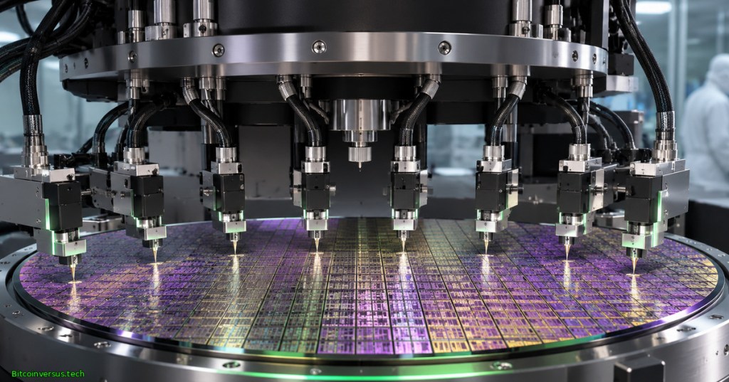
A new eight-head atomic force microscope could help semiconductor factories inspect more locations on a silicon wafer simultaneously. South Korean startup Multiscale Instruments (MSI) has developed the Chronos V8 prototype, according to a November 4, 2026 interview with founder Wonho Jhe. The instrument is not yet a verified high-volume manufacturing deployment; a formal introduction is planned for 2027.
Atomic force microscopy, or AFM, uses a sharp probe and sensitive force detection to measure surface height at nanometer and sometimes sub-nanometer scales. Unlike a conventional top-down image, the resulting height map can quantify steps, roughness, trenches and surface defects. The National Institute of Standards and Technology identifies AFM as a reference method for traceable nanoscale geometry and calibration. A semiconductor metrology primer explains how inspection data feeds process control.
Eight probes, not eight times the wafer output
The principal measurable difference is head count: eight simultaneous measurement positions versus one for the single-head baseline described by MSI. The ratio is 8 ÷ 1 = 8× as many nominal probe heads. It does not establish an eightfold gain in scans per hour, wafer throughput, yield or measurement accuracy. Travel, alignment, calibration, scan duration, site selection and tool availability all affect actual production capacity.
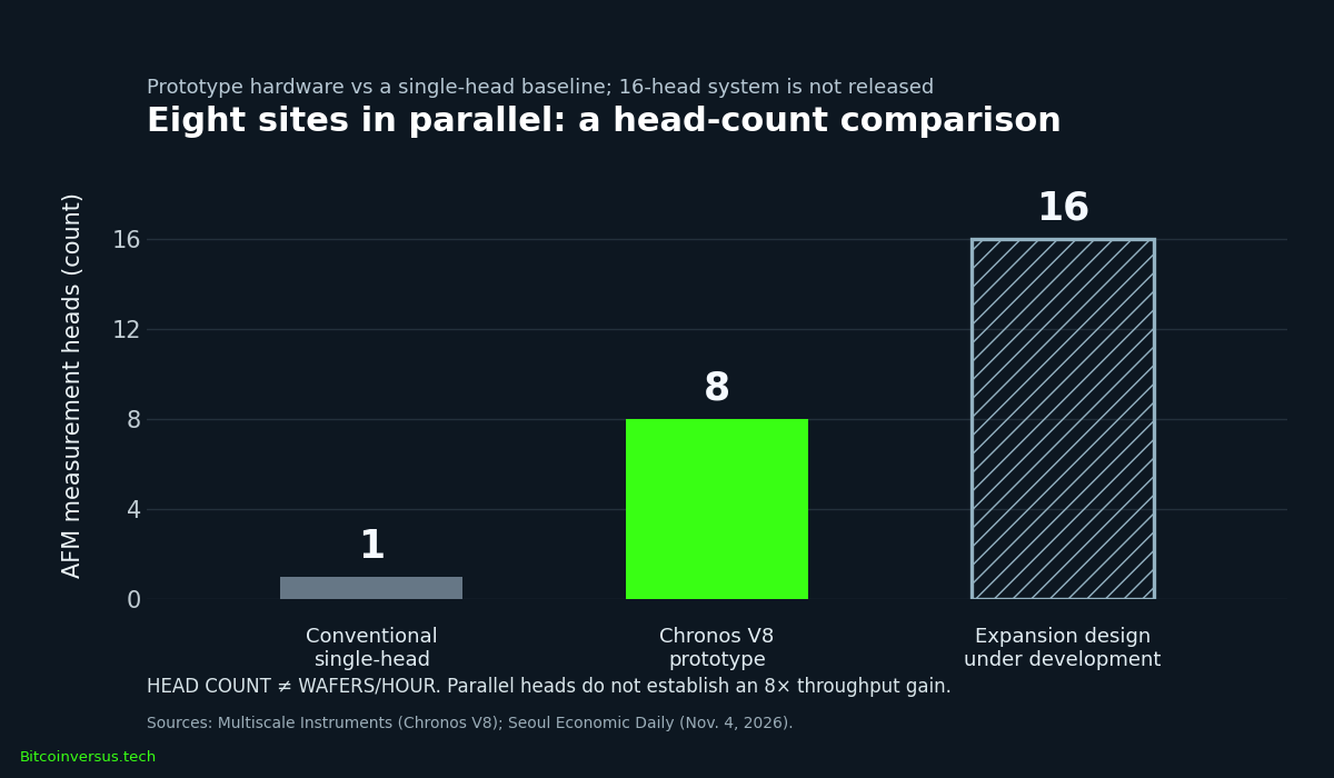
MSI describes its Chronos V8 product as a parallel, quartz-tuning-fork AFM for a 12-inch wafer, with 16-head scalability still under development. Jhe also discussed a possible 32-head architecture, but no independently verified 32-head tool performance was disclosed. The distinction matters on a 300-millimeter wafer, where fabs must sample many different die locations without slowing production.
How quartz sensing changes the design
Conventional cantilever AFM often measures probe deflection using a laser and optical detector. MSI’s quartz tuning-fork approach uses a self-sensing resonator, potentially reducing some optical readout hardware around each head. Fewer readout components may make parallel instrument design easier, but they do not eliminate every optical alignment component from a complete tool. No independent comparison of total tool size, defect-detection accuracy or lifetime cost was available in the November announcement.
AFM is complementary to—not a wholesale replacement for—optical inspection and scanning electron microscopy. Optical systems survey large areas quickly, while electron-beam instruments resolve fine pattern detail. AFM provides physical surface-height information, but tip geometry can distort widths, inaccessible sidewalls can remain challenging, and a poorly controlled probe can alter delicate samples. NIST specifically highlights calibration and measurement uncertainty as essential to interpreting nanoscale process data.
The factory test is still ahead
The latest reported financing is 4.5 billion South Korean won in Series A backing, according to Seoul Economic Daily, with a planned product introduction at CES 2027. MSI also lists an in-line high-volume version, Chronos HVX8, as a research-and-development effort targeted for the second half of 2027. Funding, a working prototype and future launch dates do not establish a qualified commercial fab installation.
Recent NIST research on AFM characterization of hybrid-bonding materials illustrates a broader manufacturing opportunity: measuring copper and dielectric behavior at scales relevant to advanced chip packaging. However, material-response measurements are different from wafer inspection throughput. A wafer-yield assessment still requires process-specific defect statistics, not merely a higher probe count.
The decisive Chronos V8 benchmarks will be wafer-per-hour throughput under a disclosed sampling recipe, repeatability and reproducibility in nanometers, false-defect rates, sample integrity, probe replacement intervals, and total operating cost. Until customers publish comparable measurements, eight-way parallelism remains an engineering capability with promising—but unquantified—factory productivity benefits.
Sources: Seoul Economic Daily, November 4, 2026; Multiscale Instruments official company site and indexed product descriptions; NIST AFM metrology; NIST 2026 hybrid-bonding study.
Editor’s Note: The eight-head prototype and Series A funding were reported in a November 4 interview; 16-head expansion and 2027 releases are manufacturer development plans, not customer-qualified output. The company’s indexed product listing could not be independently opened during final review. No eightfold wafer-throughput claim is made. The cover is conceptual artwork, not a photograph of Chronos V8 hardware. The Park Systems video illustrates another manufacturer’s AFM system. Independent playback and mobile/desktop visual inspection are not confirmed.
Support BitcoinVersus.Tech
Support independent reporting through an optional 5,000-satoshi donation using the original approved QR code below. On mobile, open the article on another screen and scan with a compatible Bitcoin wallet, or use a supported scan-from-image feature. Verify the receiving address and payment amount before sending.

We volunteer daily to ensure the information on this platform is Verifiably True. If you would like to support the research, please scan QR code.


Leave a Reply