November 8, 2026 — Silicon, graphene, diamond and photonics are often described as rivals for the next generation of computer chips. But only three are materials; photonics describes devices that manipulate light, frequently built from silicon. Their most likely outcomes between 2027 and 2040 differ by engineering function. Silicon remains the strongest candidate for mass-market processor logic; photonics leads optical communication; synthetic diamond targets heat; and graphene competes for specialized electronic layers.
A semiconductor transistor controls electric current using a channel and gate. Optical interconnects carry data as light instead of electrical signals, while heat spreaders conduct energy away from hot dies. No single benchmark fairly ranks all four functions. The forecast below concerns adoption by application, not fabricated market-share projections.
2027–2030: Silicon retains the processor
TSMC’s July 2026 earnings discussion placed second-generation nanosheet A14 risk production in 2027 and volume production in 2028. Its 2026 roadmap also targets A13 and A12 in 2029. A14’s projected 25–30% lower power at the same speed, relative to N2, is a company design target, not a field-measured 2030 efficiency gain. Years of fabrication investment and extensive chip-design libraries give silicon a major manufacturing advantage.
Meanwhile, Tower and Innolight’s early optical-device production shows where photonics can advance sooner: near processors and switches, reducing long high-speed electrical paths. NVIDIA has demonstrated co-packaged optics, but optical switches still depend on electronic control and supporting semiconductor dies.
NVIDIA’s official August 26, 2025 demonstration of Quantum-X co-packaged photonics. Source: NVIDIA/YouTube; the video shows networking, not a photonic replacement CPU.
2031–2035: Diamond and graphene seek specific layers
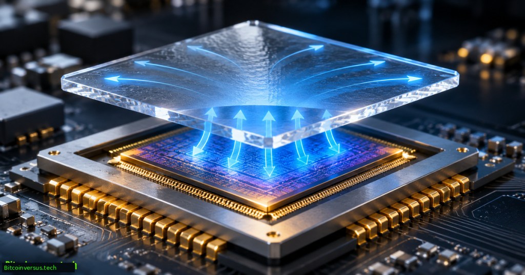
On November 3, 2026, Entegris and Element Six announced a collaboration to integrate synthetic, laboratory-grown diamond into semiconductor packages. Diamond is not replacing the silicon transistor in the announced program; it is proposed as a bonded heat-spreading layer. Commercial production timing, qualification yield and package-level temperature gains remain undisclosed.
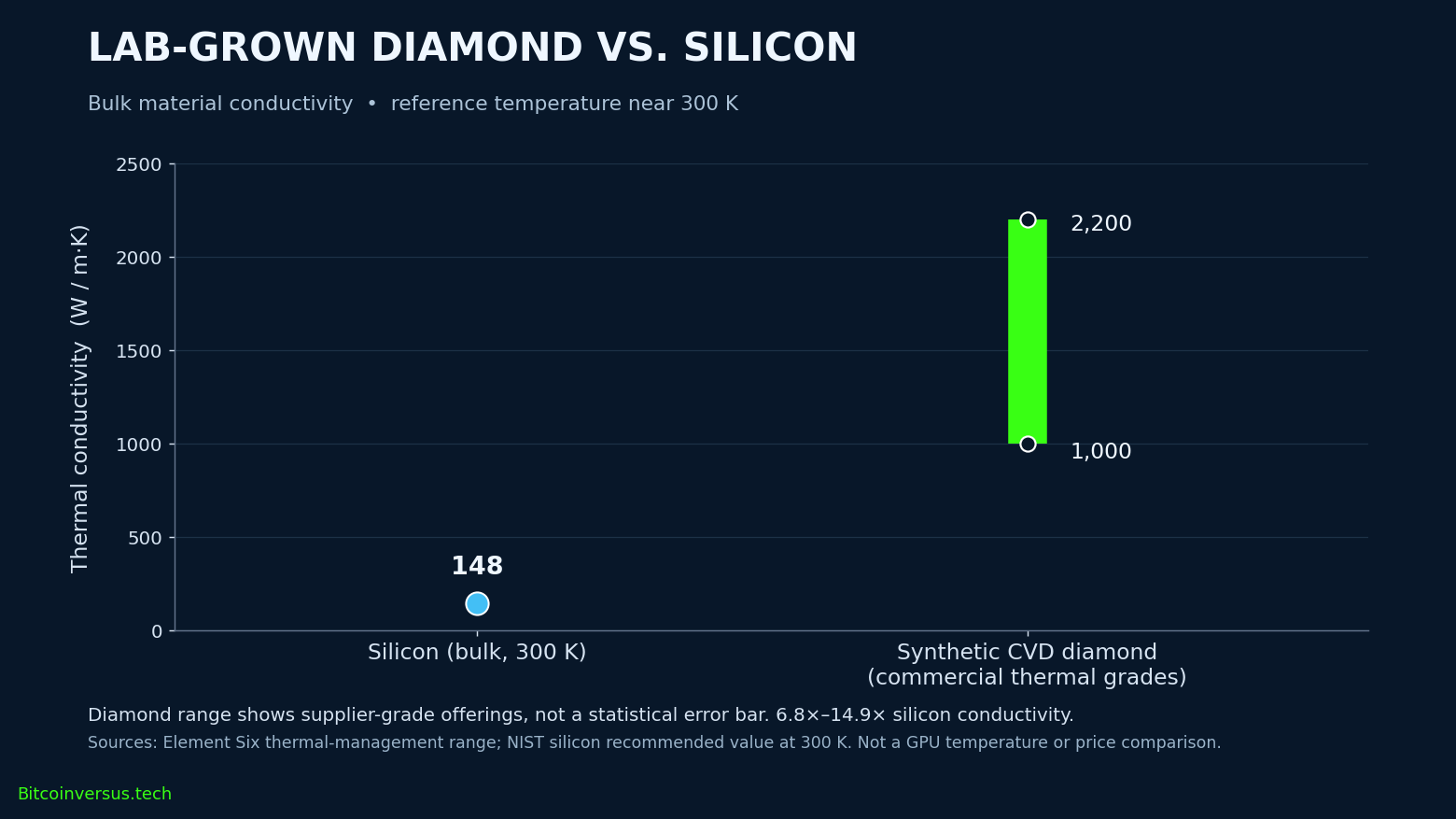
Element Six lists chemical-vapor-deposited diamond products with thermal conductivity of 1,000–2,200 W/(m·K). A published reference value for bulk silicon at 300 K is about 148 W/(m·K). The material-property ratio is 6.8–14.9×, calculated as 1,000 ÷ 148 and 2,200 ÷ 148. It is not a 6.8–14.9× prediction for GPU cooling, because bond interfaces, geometry, grade and contact resistance can dominate package performance. A separate BitcoinVersus.Tech study examines diamond manufacturing economics.
Graphene’s attraction is high electronic mobility and an atomically thin structure. Ordinary graphene lacks a useful intrinsic bandgap for digital switching. A Georgia Tech–Tianjin University 2024 Nature paper demonstrated semiconducting epitaxial graphene on silicon carbide with a 0.6 eV bandgap and room-temperature mobility above 5,000 cm²/(V·s). The measured material properties matter, but they do not demonstrate mass-market CPU yield or economics.
Official Georgia Tech video introducing the 2024 semiconducting-graphene research. Source: Georgia Tech/YouTube; research demonstration, not commercial processor production.
2036–2040: Hybrid chips are the leading scenario
By the late 2030s, the more credible direction is heterogeneous integration: silicon logic, optical I/O, improved thermal materials and selected two-dimensional channels or contacts. Graphene may appear in sensors, radio-frequency devices or supporting layers before general-purpose logic. Other 2D materials, notably MoS₂, may be better candidates for some future transistor channels; earlier BitcoinVersus.Tech coverage explains the distinction.
Can silicon be completely replaced? In a specialized component, certainly: silicon carbide and gallium nitride already serve power-electronics niches. Across mainstream CPUs, GPUs, memory-adjacent control logic and semiconductor manufacturing by 2040, a total displacement is highly improbable. Photonics is not necessarily non-silicon, graphene has integration barriers, and diamond’s strongest near-term value is thermal rather than digital logic.
The verdict is therefore silicon for computation, photonics for connectivity, synthetic diamond for thermal management, and graphene for high-upside specialized devices. Watch qualified wafer yields, cost per functional die, package thermal resistance, optical energy per transmitted bit and production shipment counts. Those measurements—not laboratory peak performance alone—will identify the real winners. See also the 2024 graphene breakthrough and the current diamond-packaging announcement.
Primary sources and methodology
TSMC A14 announcement (April 2025), Element Six announcement (November 3, 2026), Element Six material specifications, silicon thermal-conductivity reference and graphene study (January 2024). Forecast windows are editorial scenarios as of November 8, 2026, not company shipment promises.
BitcoinVersus.Tech Editor’s Note: We distinguish experimental demonstrations, production targets and verified commercial products. Material conductivity does not establish packaged-device efficiency. The accompanying chart was first prepared for a related silicon–diamond analysis; the two videos provide research and networking context. Embedding and playback require independent live checks.
Support BitcoinVersus.Tech
To make an optional 5,000-satoshi donation, scan the approved BitcoinVersus.Tech QR code using a compatible Bitcoin wallet. On mobile, open the QR on another screen or use a wallet’s supported image-scanning function. Verify the destination and amount before sending.

We volunteer daily to ensure the information on this platform is Verifiably True. If you would like to support the research, please scan QR code.


Leave a Reply