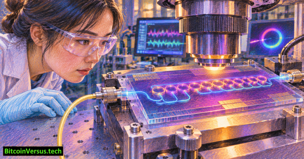
A chip developed at Carnegie Mellon University has translated electrical activity from mouse brain tissue into light without adding fluorescent dyes or genetically modifying neurons. Announced on November 20, 2026, the experimental sensor combines a one-atom-thick layer of graphene with optical microresonators. Researchers demonstrated a 20-microvolt detection limit in benchtop testing and recorded signals from 10 sensors sharing a single optical waveguide. The university announcement and peer-reviewed Advanced Science study describe a laboratory platform, not a commercial human implant.
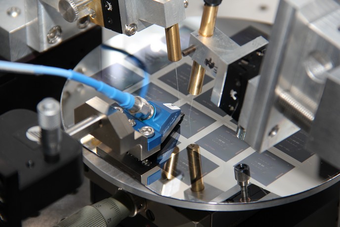
How does graphene turn voltage into an optical signal?
Neurons communicate through electrical activity that changes the voltage in surrounding tissue. At the interface between an electrolyte and graphene, charged ions form a thin electrical double layer. Tiny voltage changes alter the graphene’s electrochemical potential, changing how strongly it absorbs light. Researchers placed graphene over a microresonator, a microscopic optical structure that concentrates particular wavelengths. The changing absorption modifies light travelling through a nearby waveguide. The resulting optical fluctuation carries information about the original electrical event.
The sensor is not reading thoughts directly or accelerating electrical activity inside neurons to light speed. It is converting a measured voltage into an optical transmission for external analysis. Our materials comparison explains why graphene’s electronic and optical properties interest semiconductor engineers.
Ten sensors, one optical channel
The architecture uses wavelength-division multiplexing. Each microresonator can respond at its own wavelength, allowing multiple sensing points to share a single optical path. A receiver can distinguish the wavelength channels rather than requiring a separate long electrical wire from every sensor. The researchers reported 10 simultaneously multiplexed sensors; projections of thousands of channels remain future engineering goals, not demonstrated capacity. Comparable wavelength management also appears in high-bandwidth photonic chips.
What the sensitivity numbers actually mean
The published 20 µV detection limit was reported with a 3-decibel signal-to-noise ratio. The team also recorded evoked electrophysiological responses in mouse brain tissue, demonstrating that measured biological signals could be represented optically. Carnegie Mellon reports sensor recovery from electrical-stimulation interference almost 25 times faster than the conventional amplifier response used for comparison. That comparison addresses recovery from artifacts, not a 25-fold increase in neuron firing speed or the efficiency of a finished brain-computer interface.
Optical transmission reduces susceptibility to electromagnetic interference along the outgoing signal path. However, coupling light, managing optical power, maintaining stable graphene contact, and dealing with biological encapsulation remain practical challenges. Long-duration implanted operation, human compatibility and clinical utility have not been established by the reported experiments.
Why the architecture could matter
Large neural interfaces become difficult to scale when every recording site requires dedicated electrical interconnects. Optical multiplexing could eventually simplify that physical burden. The idea differs from biological computing systems that grow neurons on silicon and complements earlier brain–computer-interface research. The underlying photonic waveguide engineering is also related to compact optical bends used in entirely different computing applications.
The next milestone is not a promised consumer headset. It is evidence that many more channels can operate reliably in tissue while meeting constraints on device dimensions, heating, safety and signal accuracy. The new experiment establishes an intriguing bridge between electrical neuroscience and integrated photonics, with important performance and clinical questions still open.
Primary research and visual sources
- Carnegie Mellon University: November 20 research announcement and experimental context
- Advanced Science / PubMed: November 18 paper, detection limit and 10-channel recording
- Published research DOI: 10.1002/advs.78585
- Carnegie Mellon: Chamanzar research laboratory and integrated biophotonics
- European Commission CORDIS: archival graphene-photonics laboratory photograph
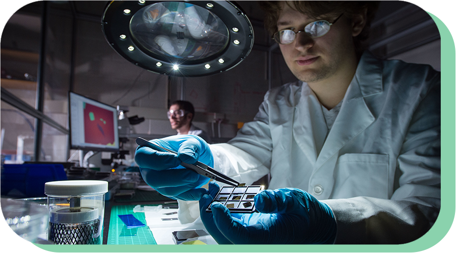
- CMU Physics: archival research laboratory photograph
- CMU College of Engineering: historical scientist interview on YouTube (external link only)
Visual disclosure: The original 1200 × 630 colored-pencil cover is conceptual, not a photo of the fabricated 2026 chip. Its saved BitcoinVersus.tech neon-green-on-black watermark was copied unmodified once at bottom-left. Two historical research photographs are captioned with their actual origins. No YouTube iframe is embedded because live playback could not be independently verified.
We volunteer daily to ensure the credibility of the information on this platform is Verifiably True. If you would like to support to help further secure the integrity of our research initiative, please scan the QR code below.



Leave a Reply