
Georgia Tech researchers have experimentally demonstrated silicon-photonic waveguide bends with a radius of just 2.3 micrometers while keeping measured optical loss extremely low and staying inside commercial foundry design rules.
The work appears in Optics Letters under the title Low-loss ultra-compact photonic bends with enhanced fabrication tolerance for commercial foundry processes. The team used topology optimization with a contour constraint designed to make the geometry both compact and manufacturable. Semiconductor Engineering highlighted the paper on October 6.
The Bend Radius Is Only 2.3 Micrometers
Waveguides are the optical equivalent of wiring inside a photonic integrated circuit. They guide light from one device to another, but tight corners are difficult: shrinking a bend too aggressively can cause light to leak out of the guide, reflect, scatter, or become sensitive to tiny manufacturing errors.
Georgia Tech’s design compresses the bend to a 2.3 µm radius. According to the published abstract, the resulting structures achieved a measured average loss of only 0.024 dB across wavelengths from 1526 nm to 1600 nm.
It Was Built On A Commercial Foundry Process
The researchers did not stop at simulation. The devices were fabricated using the GlobalFoundries Fotonix process, making the result more relevant to real chip production than a design that only works in an idealized research geometry.
That connection matters because BitcoinVersus.Tech has been following the rapid expansion of silicon photonics from multiple angles, including SMART Photonics and GlobalFoundries combining InP with silicon photonics, JEDEC’s first silicon-photonics reliability standard, and Broadcom pushing co-packaged optics into 102.4 Tb/s AI networking.
The Design Is More Tolerant Of Etching Errors
One of the harder problems in advanced photonics is that a design can look excellent on a computer and then degrade when lithography or etching shifts a feature by only a few nanometers. The Georgia Tech team specifically optimized for fabrication tolerance rather than maximum theoretical performance alone.
The paper reports robustness to both over-etch and under-etch conditions, with phase sensitivity measured at about 1.1 degrees per nanometer of waveguide-width change. The authors attribute the performance to behavior resembling whispering-gallery modes, where light follows the curved boundary efficiently instead of radiating away at the corner.
Why Smaller Bends Matter
Photonic chips are becoming more complex as engineers pack modulators, couplers, lasers, detectors, filters, switches, and optical routing onto the same die or package. Every large-radius waveguide bend consumes area that cannot be used for another device.
Reducing bend size without increasing loss lets designers route optical paths more tightly. That can improve integration density in optical interconnects, chiplets, sensors, quantum photonics, and other systems where light must travel through increasingly crowded layouts.
The same density problem appears in the broader AI hardware stack. Lightmatter is already pushing denser optical interconnects between AI chips, while foundries are trying to make photonic devices behave more like standard semiconductor building blocks that engineers can design, verify, manufacture, and scale.
The Important Part Is Manufacturability
A 2.3 µm bend would be less useful if it required exotic fabrication or failed ordinary foundry checks. The stronger result here is the combination: compact geometry, low measured loss, fabrication tolerance, and compliance with a commercial silicon-photonics process.
That is the direction integrated photonics needs to move if optical components are going to scale from specialized demonstrations into dense, repeatable semiconductor products.
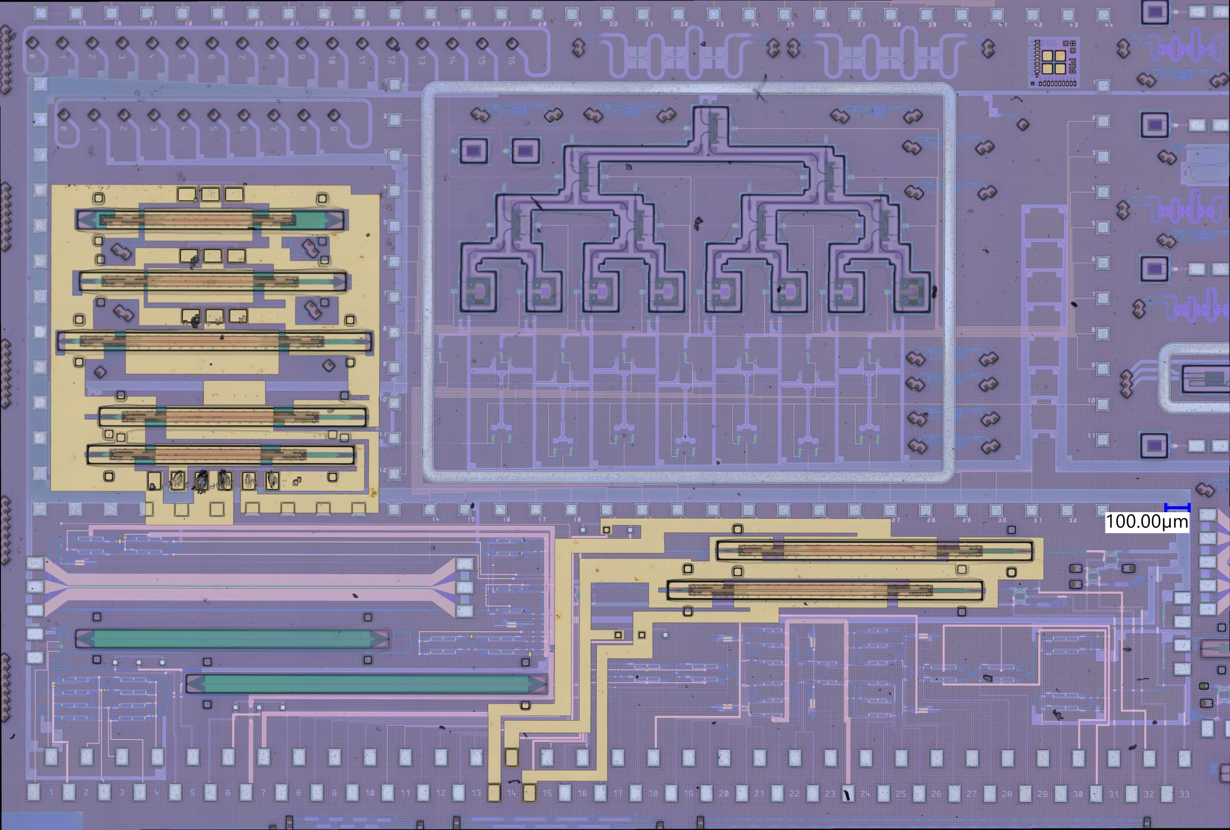
Editor’s Note
The featured image is original artwork created specifically for this story in a photorealistic editorial style and is not reused in the body. The body image is a separate silicon-photonics die micrograph from imec. The YouTube video is a responsive native Gutenberg player, and the Reddit discussion is embedded directly in the article. No normal story text is placed inside cards, panels, callouts, or text boxes.
BitcoinVersus.Tech content is provided for informational and educational purposes.


Leave a Reply