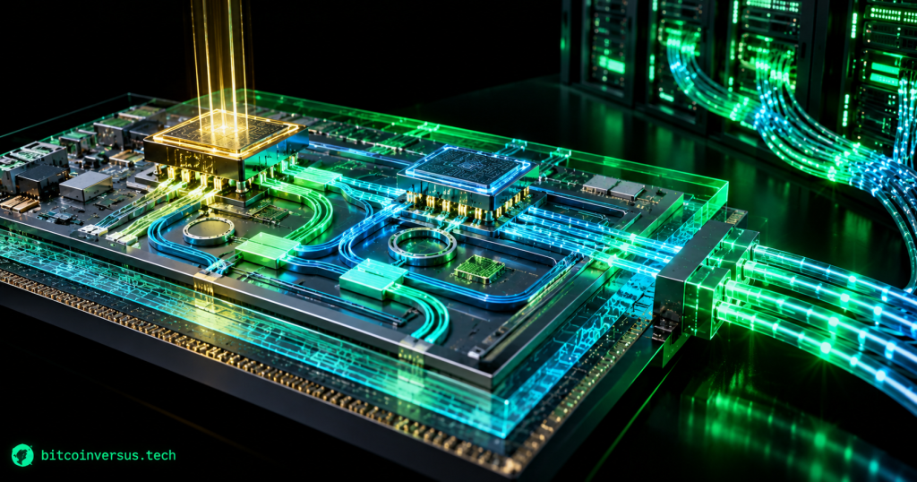
SMART Photonics and GlobalFoundries are building a new foundry route for photonic chips that combines the manufacturing scale of silicon with the active optical properties of indium phosphide.
In the September 21 announcement, the companies said the service will combine GlobalFoundries’ silicon photonics platform with SMART Photonics’ high-volume indium phosphide photonic integrated circuits, including active emitters and modulators. The target markets include AI data centers, pluggable optical transceivers, LiDAR and other optical systems.
Silicon and Indium Phosphide Solve Different Problems
Silicon is extremely useful for routing and modulating light, and it benefits from mature semiconductor manufacturing. Indium phosphide complements it by providing active optical functions that silicon does not perform efficiently on its own.
Industry analyst Neil Shah highlighted that tradeoff in a recent X analysis of the partnership, noting that the new foundry flow gives fabless optics designers a path to both materials without building the compound-semiconductor integration process themselves.
The Two Platforms Meet Through Flip-Chip Integration
GlobalFoundries provides a silicon-based cavity, while SMART Photonics supplies InP active devices and semiconductor optical amplifiers. Those components are placed into the silicon platform using flip-chip integration.
The companies say they spent more than a year co-engineering the process around dimensional fit and efficient optical coupling. That work matters because hybrid photonics only becomes useful at scale if the optical alignment and packaging process can be repeated reliably in production.
Semiconductor Today independently reported the same architecture: SMART Photonics’ InP active components are integrated into GlobalFoundries’ silicon cavity, with the companies targeting AI data-center links and pluggable optical modules.
Why AI Data Centers Need This
AI clusters are forcing more data across shorter distances between accelerators, switches and memory systems. Electrical links consume more power and become harder to scale as bandwidth rises, which is why optical connectivity is moving deeper into the data-center architecture.
BitcoinVersus.Tech recently covered how JEDEC created its first reliability standard for silicon photonics in AI networks. Standards work is one sign that these optical technologies are moving out of isolated demonstrations and toward production infrastructure.
The Foundry Model Could Matter as Much as the Device
The technical idea is not simply to prove that an InP active device can be attached to silicon. The commercial goal is to make that integration available through a foundry service so designers can build products without owning every manufacturing step themselves.
That open-access model could reduce time to market for optical-chip startups and system companies that need integrated light sources but do not want to build a dedicated compound-semiconductor manufacturing stack.
The same trend is visible in Marvell’s push toward 2 nm optical DSPs and 3.2T AI networking. The bandwidth problem is creating demand not just for faster optical components, but for manufacturing ecosystems that can assemble those components at scale.
GlobalFoundries Is Expanding the Optical Stack
The SMART Photonics partnership also fits GlobalFoundries’ broader strategy around data-center connectivity. Its expanded work with Marvell is increasing U.S. capacity for silicon-germanium technology used in next-generation optical modules, near-packaged optics and co-packaged optics.
BitcoinVersus.Tech previously examined that GlobalFoundries-Marvell capacity expansion for AI optical networking. The new SMART Photonics relationship adds a different piece of the stack: active InP photonics integrated with silicon through a coordinated foundry flow.
General Availability Is Targeted for the Second Half of 2027
The service is not generally available yet. SMART Photonics and GlobalFoundries are targeting the second half of 2027 for broad availability.
That gives the companies time to turn their co-engineered integration process into something designers can repeatedly use through a commercial foundry model. The key milestone will be whether customers can move from design to volume optical products without recreating the integration process themselves.
BitcoinVersus.Tech
Advertisement
Editor’s Note:
We volunteer daily to ensure the credibility of the information on this platform is Verifiably True. If you would like to support our research initiatives, please donate here: 3C9o19EH5HSiwEPyCTmEKzxhNCbo2X6TTb
BitcoinVersus.tech is not a financial advisor. This media platform reports on financial subjects purely for informational purposes.


Leave a Reply