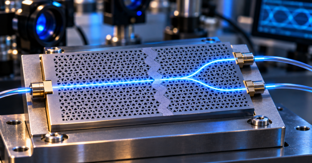
India’s Ministry of Science and Technology announced November 4, 2026, that researchers demonstrated up to 100 gigabits per second of terahertz data transmission through an engineered barrier on a silicon photonic chip. The experiment took place at the Jawaharlal Nehru Centre for Advanced Scientific Research (JNCASR), with collaborators in India, Singapore and France. The result concerns laboratory-scale guided terahertz signals, not a deployed 6G cellular network.
The peer-reviewed research, published October 11 in Advanced Materials, reports a silicon topological photonic crystal engineered with triangular holes. The geometry allows an electromagnetic signal to travel along a protected interface, cross a deliberately introduced obstacle and continue with comparatively little loss. The effect is known as photonic Klein tunnelling, referring to a wave analogue of a phenomenon in quantum physics.
NPTEL / IIT Guwahati, “Simulation Demonstration of Topological Photonic Crystals Based Waveguides (Part 1),” March 2025. Official university lecture on the physics behind topological waveguides; not footage of JNCASR’s experiment.
A silicon lattice designed to carry terahertz signals
A photonic crystal is a material patterned to alter how electromagnetic waves propagate. Here, two regions of high-resistivity silicon contain a honeycomb-like arrangement of triangular holes. Their boundary creates a path for terahertz radiation. Adjusting the sizes of holes over a short region changes its effective barrier strength, letting researchers test whether the wave keeps propagating rather than reflecting or scattering away.
Measurements covered 310–360 gigahertz, corresponding to frequencies far above conventional cellular radio bands. A single engineered barrier added about 1–2% transmission loss, while two barriers introduced approximately 2–3% relative to the baseline, according to the government report. The results held within a particular range of engineered barrier strengths; the researchers did not demonstrate immunity to arbitrarily large obstacles.
Such robustness could eventually make compact terahertz routing components easier to design. Related topics appear in BitcoinVersus.Tech reporting on micrometer-scale silicon photonic bends and silicon photonics reliability requirements. Those projects concern different frequencies, applications and fabrication technologies.
Three devices, three different data rates
The researchers fabricated three configurations. A structure containing two barriers carried 48 Gbit/s, while an omega-shaped path with four sharp bends and a central barrier carried 60 Gbit/s. A separate power-splitter design transmitted data at 100 Gbit/s using 32-state quadrature amplitude modulation, or QAM-32, which encodes information through variations in carrier amplitude and phase.
The headline 100 Gbit/s figure therefore belongs to the splitter experiment; it is not the measured speed of every chip layout. At 100 gigabits per second, a theoretical 5-gigabyte file contains approximately 40 gigabits, corresponding to 0.4 seconds of idealized transfer time. Protocol overhead, coding, conversion and practical hardware would add time. The experiment also does not establish equivalent wireless throughput between phones or cellular towers.
NPTEL / IIT Guwahati, “Simulation Demonstration of Topological Photonic Crystals Based Waveguides (Part 2),” September 2024. University teaching material provides supporting simulation context; it predates and does not depict the reported chip tests.
Promising physics, unresolved engineering
The published scientific abstract reports that valley pseudospin was preserved by more than 98% across two cascaded barriers, helping quantify the intended topological behavior. The authors also identify a limit: transmission deteriorates when barrier strength approaches a characteristic coupling energy in the lattice. Their experiments demonstrate a controllable design principle, not a lossless circuit under every condition.
Future 6G systems might use high-frequency interconnects to route signals between chips, antennas or communication modules. Commercial use would still require compatible terahertz sources and receivers, packaging, efficient power consumption, temperature stability and repeatable fabrication yields. Related outdoor 6G field demonstrations and AI-native 6G network research address separate system-level problems; neither proves the JNCASR structure can be integrated into a complete radio.
The team led by Abhishek Kumar next proposes electrically, mechanically or thermally tuning the barriers, potentially creating dynamically reconfigurable routing paths. The immediate achievement is narrower but concrete: fabricated silicon devices guided terahertz data through selected obstacles at verified laboratory speeds. Independent replication, system integration and field measurements remain future milestones.
Editor’s Note: Primary research is Mulla and colleagues, Advanced Materials, published October 11, 2026; reported device measurements and research-team details were cross-checked against India’s November 4 science-ministry release. The 100 Gbit/s maximum applies to the splitter configuration, not each device or a public 6G network. The featured cover is original conceptual artwork rather than a lab photograph, and both IIT Guwahati lectures predate the paper.

For mobile scanning, open the article on another display and scan the original QR with a compatible Bitcoin wallet. Verify the destination before donating 5,000 sats: 3C9o19EH5HSiwEPyCTmEKzxhNCbo2X6TTb.
We volunteer daily to ensure the credibility of the information on this platform is Verifiably True. If you would like to support our work and help further secure the integrity of our research initiatives, please scan the QR code below to donate 5,000 sats.
BitcoinVersus.tech is not a financial advisor. This media platform reports on financial subjects purely for informational purposes.


Leave a Reply