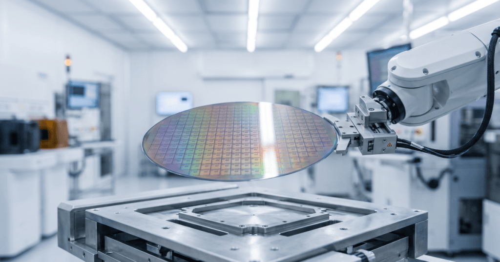
A 300 mm wafer is a circular slice of semiconductor material that measures 300 millimeters across its diameter. That is 30 centimeters, or about 11.81 inches, which is why the industry often calls it a 12-inch wafer.
The key word is diameter: 300 mm is the straight-line distance from one edge of the wafer to the opposite edge through the center. The radius is only 150 mm. The number does not describe the wafer’s length, thickness, or the size of an individual chip.
A Wafer Is the Starting Platform, Not the Finished Chip
A wafer is the flat platform on which a chip factory builds many semiconductor devices at the same time. Most high-volume chips start on silicon. Repeated layers are deposited, patterned, etched, doped, cleaned, measured, and inspected until hundreds or thousands of individual rectangular chip areas, called dies, cover much of the circular surface.
ASML’s manufacturing overview notes that 300 mm is the wafer size most often used in semiconductor manufacturing and that a finished wafer can contain anything from only a few dozen large dies to thousands of smaller ones. The complete manufacturing flow can involve thousands of process steps before those dies are separated.
Why 300 mm Became So Important
The basic advantage is simple geometry: a bigger circle gives a factory more surface area to process in each wafer cycle. A 300 mm wafer has an area of about 70,686 mm², while a 200 mm wafer has about 31,416 mm². That is roughly 2.25× more raw area.
Real die output does not scale perfectly with area because chip rectangles do not tile the curved wafer edge perfectly, some edge area cannot be used, and defects can reduce the number of good dies. Even so, when Applied Materials introduced a broad 300 mm equipment lineup in 2000, it said the move from 200 mm to 300 mm could allow up to about 2.5× more chips on a wafer depending on the product and process.
Why More Dies Per Wafer Can Lower Cost
A semiconductor fab performs expensive operations on an entire wafer: lithography, deposition, etch, ion implantation, cleaning, metrology, inspection, and thermal processing. If one wafer carries more potential dies, more chips can share the cost of those wafer-level operations.
That does not mean every 300 mm wafer is automatically cheap. The number of sellable chips still depends heavily on wafer yield: how many dies actually pass electrical and functional testing. A wafer packed with defects can have more physical die locations yet produce fewer useful chips.
How Lithography Uses the Wafer
Lithography does not normally print one giant 300 mm image across the wafer. A scanner repeatedly exposes smaller fields while the wafer stage moves with extreme precision. The process repeats across the circular surface, layer after layer, while alignment systems keep new patterns registered to structures already built below.
That same basic idea continues into the most advanced production systems. BitcoinVersus.Tech’s look at ASML High-NA EUV moving into chip production shows how much engineering sits between a blank wafer and an advanced logic die: optics, reticles, wafer stages, overlay control, resist chemistry, metrology, and process integration all have to work together.
A 300 mm Wafer Is Bigger Than the Chip You Buy
The finished processor, memory chip, sensor, or ASIC inside a product is usually only one small rectangle cut from the wafer. Before cutting, the factory can electrically test dies while they are still attached to the wafer. Afterward, a dicing process separates the good dies so they can move into assembly and packaging.
Packaging then turns a fragile bare die into something that can connect to a circuit board, remove heat, deliver power, and move signals. The semiconductor packaging flow is therefore the next major stage after wafer fabrication and dicing.
Why Fabs Need Specialized 300 mm Equipment
A 300 mm wafer is large enough that high-volume factories depend heavily on automated handling. Robots move wafers between carriers, load ports, process chambers, measurement tools, and lithography systems while trying to avoid particles, scratches, vibration, alignment errors, and contamination.
The wafer may look simple—a thin, shiny circle—but the factory surrounding it is one of the most precise manufacturing environments on Earth. Every major tool has to know where the wafer is, where each field is located, what process has already been completed, and what comes next.
The Simple Way to Remember It
300 mm means the wafer is 300 millimeters across. That is about 30 centimeters or 11.81 inches. The wafer is not one giant chip; it is a manufacturing platform that can hold many dies while the fab builds their microscopic structures in parallel.
The larger wafer gives manufacturers more usable surface area per processing cycle, but the economics still depend on die size, process complexity, equipment productivity, and yield. That combination—not diameter alone—is what determines how many working chips eventually leave the fab.
BitcoinVersus.Tech
Advertisement
Editor’s Note
Wafer dimensions, edge exclusions, die counts, process flows, and yields vary by manufacturer and technology. The figures here are simplified to explain the geometry and manufacturing logic behind the common 300 mm format.
Support and donation options are available through BitcoinVersus.Tech.
BitcoinVersus.tech is not a financial advisor. Content is provided for informational purposes.


Leave a comment