Artificial-intelligence infrastructure is creating a new kind of materials story: the faster companies build AI data centers, the more tin they need to physically connect the hardware inside them.
Tin is not doing the computing. GPUs, CPUs, memory, networking silicon, and optical devices do that. But tin-based solder is one of the materials that electrically and mechanically joins those components to circuit boards, packages, connectors, and modules. That makes a relatively old industrial metal newly important to the AI buildout.
Reuters reported on October 7 that London Metal Exchange tin has traded above $50,000 per metric ton since June 2026 after more than doubling over three years. The same report pointed to AI infrastructure, electric vehicles, and constrained supply as important forces behind the change.
Why Tin Is Everywhere Inside Electronics
The core use is solder. Modern electronics rely on thousands of small joints that connect chips, resistors, capacitors, connectors, memory packages, power devices, and other components to printed circuit boards. Tin is especially useful because it melts at a relatively low temperature and forms reliable electrical and mechanical joints with copper and other conductors.
The International Tin Association says solder remains the largest use of tin globally. Its broader technology overview describes tin as the “glue” connecting electronics, from circuit boards and wiring to renewable-energy hardware.
AI Servers Use More Tin Than Traditional Servers
The shift is not simply that more servers are being built. AI systems are also becoming more electrically dense. Shanghai Metals Market estimates that a traditional server uses about 0.5 kilograms of tin while an AI server can use roughly 4 to 5 kilograms. SMM attributes the increase to larger and more complex boards, denser interconnects, advanced memory packaging, and faster optical modules.
That hardware stack is familiar across BitcoinVersus.Tech’s coverage. Modern accelerators pair powerful compute dies with HBM, advanced semiconductor packaging, high-density substrates, voltage-regulation hardware, and increasingly complex server motherboards.
SMM says the motherboard area of high-end AI servers can reach three to five times that of traditional machines, with board layer counts rising into the 16-to-30-layer range in some designs. More layers and more components mean more solder joints.
HBM Adds Another Layer of Solder Density
HBM4 and other stacked-memory technologies increase interconnect density around AI processors. SMM says the micro-bump count between a high-end GPU and HBM can reach into the hundreds of thousands, with tin-based solder used across many of those microscopic connections.
This is one reason the industry’s push toward 2.5D and 3D packaging, chiplets, interposers, and stacked memory matters beyond the silicon itself. The package becomes a dense electrical system in its own right.
BitcoinVersus.Tech has also tracked shortages in the less-visible materials around AI chips, including the specialty glass cloth inside advanced chip substrates. Tin fits the same pattern: the AI boom is pulling demand through parts of the hardware supply chain that rarely appear on a GPU specification sheet.
Optical Networking Still Needs Solder
AI clusters also need enormous amounts of high-speed networking. Even as the industry moves more data through fiber and photonics, the optical modules themselves still contain electronics, lasers, drivers, detectors, connectors, and small circuit boards that must be assembled and electrically connected.
SMM specifically points to 800G and 1.6T optical modules as another source of ultra-fine solder demand. That connects directly with the move toward 1.6T AI optics and eventually denser co-packaged optical systems.
The same scale-up is reshaping the physical network around the racks. BitcoinVersus.Tech has covered both AI data-center cabling and top-of-rack switches, two examples of how faster compute creates more demand for connectivity hardware around the processors themselves.
How Much Tin Does a Gigawatt of AI Capacity Need?
SMM estimates that each gigawatt of installed AI data-center capacity can require roughly 1,200 to 1,500 metric tons of tin across servers, GPUs, networking equipment, control systems, cooling hardware, and other infrastructure. Reuters highlighted the same estimate in its October 7 analysis.
That number should be treated as an industry estimate rather than a universal engineering constant. A data center can use very different server architectures, rack densities, network designs, cooling systems, and power topologies. But the direction is clear: more installed AI hardware means more board-level interconnections.
SMM estimates that PCB board-level soldering accounts for roughly 85% to 92% of tin use in AI computing centers, while power-distribution hardware represents less than 1%. In other words, tin’s main job is connection, not bulk power transmission.
The Power System Still Matters—Just Differently
The fact that solder dominates tin use does not make the electrical infrastructure unimportant. AI campuses still need transformers, switchgear, UPS systems, busway, rack PDUs, generators, cooling systems, and network equipment.
Those systems are being deployed at a time when U.S. electricity demand is also rising. BitcoinVersus.Tech recently covered the record power demand expected from AI and crypto data centers. Tin demand is a different part of the same buildout: one story is about supplying megawatts, the other is about physically connecting the electronics that consume them.
Hybrid Bonding Could Reduce Some Tin Use
There is one important long-term countertrend. Hybrid bonding can connect dies using direct copper-to-copper interfaces instead of relying on solder micro-bumps in some advanced packaging steps.
SMM expects that technology to reduce tin demand in parts of advanced packaging after 2030, but not to eliminate the much larger board-level solder market. Even if chip packages use fewer solder bumps, motherboards, optical modules, connectors, and other assemblies still need reliable electrical joints.
Tin Supply Is Not Expanding as Fast as the Story
Demand is only half of the equation. Reuters reported that combined visible stocks registered with the London Metal Exchange and Shanghai Futures Exchange fell from about 22,600 tons in February 2026 to roughly 13,100 tons by early October.
The International Tin Association has separately warned that long-term technology demand will require new investment in mine supply. Its 2026 investment materials say tin demand could rise about 25% by 2035 and describe historic underinvestment in new production as a supply challenge.
The Bigger Hardware Lesson
The AI infrastructure race is usually described with headline components: GPUs, CPU cache, HBM, optical links, power generation, and cooling. But every generation of compute also depends on ordinary-looking materials that make the entire system manufacturable.
Tin solder is one of those materials. A server can have the fastest CPU and GPU roadmap in the world, but it still needs thousands of dependable electrical joints to turn those chips into a working machine.
That makes tin a useful reminder of how the AI boom really works: progress at the top of the stack creates demand all the way down through silicon wafers, packaging, substrates, memory, circuit boards, solder, cables, racks, and power systems.
Editor’s Note
SMM’s AI tin-consumption figures are industry estimates and will vary by architecture, hardware mix, rack design, and data-center configuration. Reuters’ October 7 article is commentary by metals columnist Andy Home, with the underlying AI hardware estimates attributed to Shanghai Metals Market.
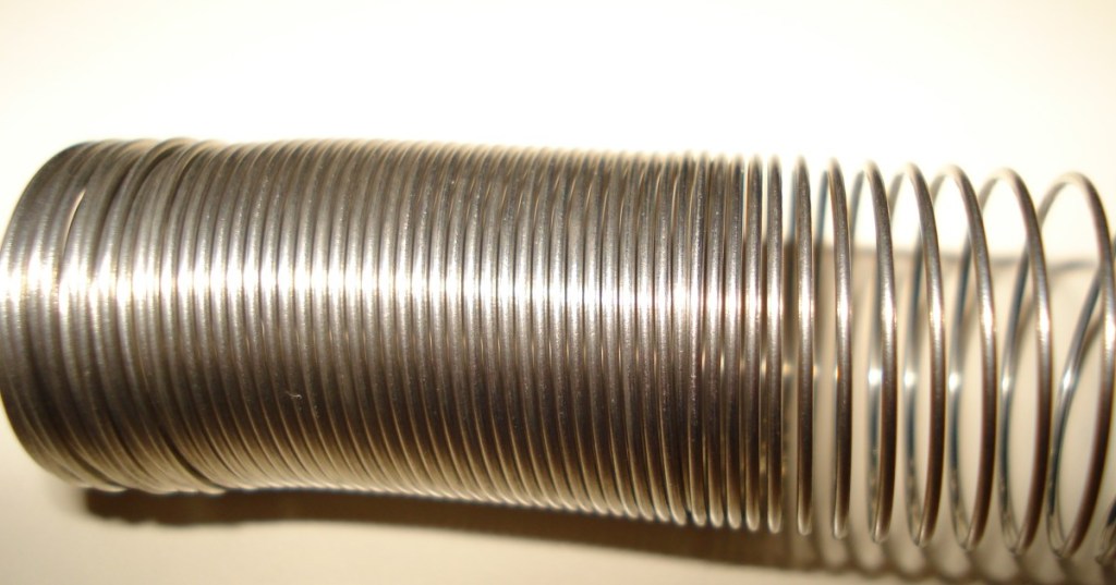
Featured image: “Pure tin solder” by Tremaster, via Wikimedia Commons, licensed CC BY-SA 3.0; cropped to 1200×630 for BitcoinVersus.Tech.
Support and donation options are available through BitcoinVersus.Tech.
BitcoinVersus.tech is not a financial advisor. Content is provided for informational purposes.


Leave a comment