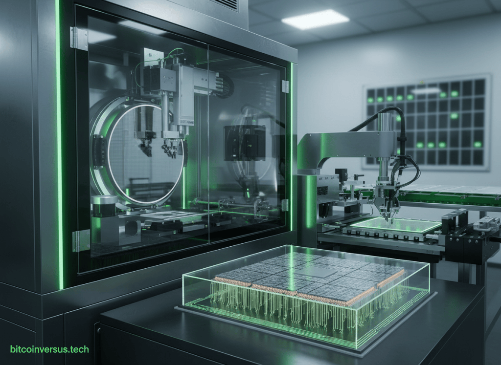
Applied Materials and BE Semiconductor Industries are expanding their chip-packaging partnership from one hybrid-bonding tool into a broader integration roadmap for AI systems. Besi is joining Applied’s EPIC Center as an Innovation Partner, where the companies plan to work on die-to-wafer hybrid bonding, thermo-compression bonding, die-on-die, die-on-panel and photonics-enabled interconnects.
The October 1 agreement matters because advanced packaging is becoming part of the performance architecture of AI chips rather than a final assembly step. In its specific announcement, Applied Materials said the expanded collaboration moves beyond the companies’ existing hybrid-bonding work into new interconnect architectures intended to support AI scaling.
Hybrid bonding removes the bump
Traditional advanced packages often connect dies through microscopic solder bumps. Hybrid bonding pushes the interconnect pitch much lower by preparing extremely flat dielectric surfaces and copper contacts, aligning the dies precisely and creating direct copper-to-copper electrical connections as the surfaces bond.
That tighter pitch can increase interconnect density while shortening the electrical path between chiplets. For AI processors, where compute dies must continuously exchange enormous amounts of data with memory and other accelerators, those shorter and denser connections can become a system-level performance advantage.
The two companies already have a working foundation. According to the Applied Materials announcement, their joint development program began in 2020 at an advanced-packaging center in Singapore. Applied contributed process technologies including etch, planarization, deposition, wafer cleaning, metrology, inspection and particle control, while Besi contributed die placement, interconnect and assembly technology.
That work produced Kinex, which Applied describes as an integrated die-to-wafer hybrid bonding system. The significance of integration is process control: cleaning, surface preparation, inspection and precision die placement all affect whether microscopic bonds form consistently enough for high-volume manufacturing.
The roadmap now extends beyond Kinex
The new collaboration broadens the engineering target. Applied and Besi say their planned R&D includes new die-to-wafer hybrid bonding platforms, further scaling of thermo-compression bonding and its surrounding process ecosystem, and new die-on-wafer, die-on-die and die-on-panel integration platforms.
Die-on-panel is particularly interesting because rectangular panels can offer a different manufacturing geometry from circular wafers. If process uniformity, alignment and yield can be controlled at larger panel scale, packaging lines could potentially assemble more heterogeneous devices per substrate. The challenge is that the precision requirements do not become easier merely because the substrate becomes larger.
The expansion fits the packaging pressure BitcoinVersus.tech recently examined in CoWoS-L’s push beyond conventional reticle limits. AI systems increasingly need more compute, memory and I/O inside one tightly coupled package, so packaging technologies are being asked to scale in dimensions that transistor shrink alone cannot solve.
Thermo-compression bonding stays in the roadmap
Hybrid bonding is not replacing every packaging method at once. Applied and Besi are also expanding work on thermo-compression bonding, or TCB, which uses controlled heat and mechanical pressure to form fine-pitch interconnects. Different chiplets, substrates, pitches and production volumes can favor different bonding methods.
That makes the partnership less about declaring one universal winner and more about co-optimizing a packaging flow. Etch, deposition, cleaning, planarization, metrology and defect control happen upstream of the placement and bonding step, but a defect in any one of those stages can determine whether an expensive multi-die package survives final test.
Photonics enters the packaging flow
The companies also plan to work on photonics-enabled interconnect applications for co-packaged optics and AI system scaling. That moves the collaboration into another fast-changing boundary: electrical links become increasingly difficult to drive efficiently as bandwidth rises, while optical links can carry high data rates over distance with different power and signal-integrity tradeoffs.
Packaging is where those domains meet. A co-packaged optical system must integrate electronic compute or switching silicon with photonic devices, optical interfaces, power delivery and thermal management while maintaining manufacturing yield. The bonding and materials stack therefore becomes part of the networking architecture.
BitcoinVersus.tech has already seen that trend from the system side in Avicena’s detachable MicroLED optical links for AI racks. Applied and Besi are approaching the problem from manufacturing: how to build the dense heterogeneous packages that future optical AI systems will require.
EPIC puts packaging beside front-end process R&D
Besi engineers will work with Applied teams at the EPIC Center in Silicon Valley. Applied’s argument is that advanced packaging now demands materials engineering, cleanliness and process control closer to front-end wafer fabrication than to conventional back-end assembly.
Independent coverage from Stock Titan similarly highlights that the partnership is expanding from its 2020 chip-bonding program into light-based links and broader AI packaging development. The key change is organizational as much as technical: equipment suppliers, logic companies, memory vendors and systems builders can test process interactions earlier rather than handing a finished wafer to packaging as a separate downstream problem.
That model also connects with Applied’s separate memory work. BitcoinVersus.tech recently covered KIOXIA joining Applied’s EPIC Center for AI memory R&D. Besi adds assembly and bonding expertise to the same broader co-development environment, but the October 1 agreement is specifically about interconnect and package integration rather than memory-device development.
The manufacturing test comes next
The partnership announcement does not provide production throughput, bond-pitch, yield or customer-volume targets for the new platforms. Those measurements will ultimately determine whether die-on-panel, next-generation hybrid bonding and photonics-enabled packaging can move from R&D into economically competitive high-volume manufacturing.
What is already clear is that AI scaling is pushing semiconductor manufacturing outward from the transistor. The package now has to connect logic, memory, chiplets and eventually optical I/O at densities high enough that the bonding equipment itself becomes part of the performance roadmap. Applied Materials and Besi are building their next collaboration around that shift.
BitcoinVersus.Tech
Advertisement
BitcoinVersus.Tech Editor’s Note:
We volunteer daily to ensure the credibility of the information on this platform is Verifiably True. If you would like to support to help further secure the integrity of our research initiatives, please donate here: 3C9o19EH5HSiwEPyCTmEKzxhNCbo2X6TTb
BitcoinVersus.tech is not a financial advisor. This media platform reports on financial subjects purely for informational purposes.


Leave a Reply