Advanced semiconductor packaging is becoming one of the most important constraints in AI hardware, and a new September 18 report says the industry is now pushing package sizes beyond traditional reticle limits. TrendForce reports that TSMC’s CoWoS-L is expected to remain the mainstream 2.5D packaging platform for leading AI chips through 2028, even as Intel’s EMIB-T and other approaches compete for share.
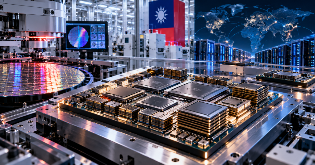
AI Chips Are Outgrowing a Single Reticle
Reticle limits come from the maximum area a lithography system can expose in one shot. As accelerator designs combine larger logic dies, multiple chiplets and high-bandwidth memory, packaging becomes the layer that lets designers assemble systems larger than any single monolithic die. TrendForce says the latest AI platforms are increasing total package area and making 2.5D integration a core performance technology rather than a final assembly step.
The supporting video comes from a verified channel with more than one million subscribers and focuses specifically on CoWoS, HBM integration and the packaging bottleneck behind modern AI accelerators. That makes it a useful companion to the newer TrendForce forecast rather than a generic semiconductor embed.
CoWoS-L Gains From Maturity and Yield
TrendForce says CoWoS-L should keep an advantage through 2028 because of manufacturing maturity and yield, even as competing architectures improve. The report points to continued growth in Nvidia’s rack-scale systems and AMD’s MI400 and MI450 families as additional pressure on advanced packaging capacity.
That trend connects directly to the memory side of the AI stack. BitcoinVersus.tech recently covered how SK hynix is preparing HBM4 for mass production, because the performance of modern accelerators depends increasingly on moving data between compute dies and stacked memory at extremely high bandwidth.
Packaging Is Becoming Part of System Architecture
The change is important because advanced packaging is no longer a passive substrate problem. Designers now have to co-optimize logic, HBM placement, interposers, thermal paths, power delivery and high-speed links as one system. Larger package footprints can increase routing flexibility and memory bandwidth, but they also raise yield, warpage, heat-density and manufacturing-control challenges.
BitcoinVersus.tech has also tracked the front-end manufacturing side of the same scaling problem, including ASML’s High-NA EUV move into production. High-NA can help shrink and pattern leading-edge logic, while CoWoS-L and competing packaging technologies determine how those dies are combined into complete accelerator systems.
Why Data Centers Should Care
For data-center operators, advanced packaging eventually shows up as rack-level reality. Package size and memory density influence accelerator power, cooling requirements, serviceability and the amount of compute that can be packed into a rack. As AI systems move toward larger integrated modules, cooling and power-delivery infrastructure must scale alongside the silicon.
The packaging race therefore sits between semiconductor fabrication and the physical data center. Faster transistors alone are not enough if manufacturers cannot economically connect compute, memory and networking silicon at the required scale. TrendForce’s 2028 outlook suggests that the next phase of AI hardware competition will be fought as much in packaging lines as in wafer fabs.
Disclaimer: BitcoinVersus.tech provides technology news and analysis for informational and educational purposes only. Semiconductor roadmaps, capacity plans and packaging forecasts can change as manufacturing yields, customer designs and product schedules evolve.


Leave a Reply