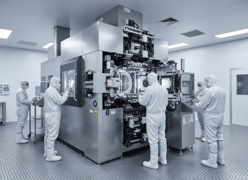
The semiconductor industry’s most advanced chipmaking machines are moving from early adoption toward broader production as ASML, Intel, TSMC and Samsung prepare the next generation of extreme ultraviolet lithography.
The technology is called High Numerical Aperture Extreme Ultraviolet lithography, usually shortened to High NA EUV. It gives chipmakers more precise patterning than today’s standard EUV systems, an increasingly important capability as AI processors and memory become denser and more complex.
Intel Is Already Using High NA
Intel Foundry has moved first. ASML and Intel said High NA is already being used in high-volume manufacturing on selected layers of Intel’s 18A process for a subset of Core Ultra Series 3 processors, code-named Panther Lake.
The companies said more than one million wafers have now passed through High NA systems across equipment certification, research, development and volume production. Intel says throughput, overlay accuracy and availability are meeting its expectations.
Samsung and TSMC Have Set Their Timelines
Samsung plans to introduce High NA EUV into high-volume DRAM manufacturing by 2028. TSMC says it intends to use the technology for high-volume manufacturing of advanced logic nodes beginning in 2030.
Those timelines matter because Samsung and TSMC manufacture enormous volumes of memory and advanced processors. Wider adoption would move High NA from an expensive early-production technology toward a standard tool for some of the world’s most advanced chips.
The Industry Wants Bigger Masks
ASML and TSMC are also leading an industry effort to move from conventional 6-inch photomasks toward larger 12-inch masks for High NA systems. A photomask contains the circuit pattern that a lithography machine projects onto a silicon wafer.
The larger format is intended to improve scanner productivity, reduce manufacturing costs and remove some stitching limitations when producing very large chips. ASML and TSMC are targeting a 12-inch mask pilot line by 2031 and production-ready lithography systems by 2033.
Why High NA Matters for AI Hardware
Modern AI accelerators depend on enormous numbers of transistors, advanced memory and increasingly complicated manufacturing. Better lithography can allow chipmakers to print smaller features with fewer patterning steps.
That does not automatically make chips cheaper. High NA machines are among the most complicated manufacturing systems ever built, and fabs must also invest in masks, materials, metrology and process changes around them.
The important development is that High NA is no longer only a laboratory technology. Intel is using it on shipping products, Samsung and TSMC have published production roadmaps, and the semiconductor supply chain is now working on the larger masks that could make the technology more useful for the enormous processors found in future AI data centers.
Sources: ASML, TSMC, Intel Foundry, Samsung Electronics and Reuters.
Related BitcoinVersus.tech coverage: Synopsys TSMC A14 · Major chipmakers evaluate Intel 14A · Tower optical chips · SK hynix AI memory
BitcoinVersus.Tech Editor’s Note: We volunteer daily to help ensure the credibility of information on this platform is verifiably true. BitcoinVersus.tech is not a financial advisor. This article is independent reporting and educational content for informational purposes only.


Leave a Reply