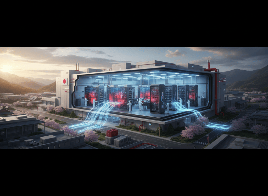
Tower Semiconductor is turning its Japanese manufacturing footprint into what is planned to become its largest optical-connectivity semiconductor hub, with new reporting putting the program at roughly $4 billion and projecting the equivalent of 45,000 300 mm wafers per month by 2029.
New details published September 24 say the expansion could lift Tower’s Japanese capacity to roughly 40 times its 2025 level. The company previously confirmed the underlying dual-track plan with Japanese government support, while earlier reporting established Tower’s planned $3 billion contribution plus $1 billion in government grants.
45,000 Wafer Equivalents Changes the Scale
The fresh number is the important part. Tower had already disclosed its Japan expansion in July. The September update provides a clearer picture of the intended manufacturing scale: the equivalent of 45,000 300 mm wafers per month by 2029, approximately 40 times 2025 output, according to current reporting.
This is not simply another fab announcement. The capacity is aimed at silicon photonics, silicon germanium and advanced optical packaging, technologies increasingly used to move data between AI accelerators, switches and data-center systems with lower power per bit than traditional electrical links.
Japan Gets a Two-Track Optical Manufacturing Buildout
Track one repurposes Tower’s former Fab 6 in Arai, Niigata Prefecture for 300 mm silicon-photonics production and advanced packaging while increasing output at Fab 7 in Uozu, Toyama Prefecture. Tower says full production readiness for this stage is expected in the fourth quarter of 2027.
Track two calls for another 300 mm manufacturing facility next to Fab 7 after the related agreements are signed and closed. That second facility is expected to add another multi-fold increase in silicon-photonics and SiGe capacity, with the new capacity becoming financially meaningful beginning in 2029.
Why AI Is Pulling Optics Into the Fab
AI clusters increasingly run into bandwidth, distance and power constraints between processors. BitcoinVersus.tech recently covered Tower and NewPhotonics moving 800G and 1.6T laser-integrated optical engines into volume shipment. That product milestone and the Japan capacity expansion are related but distinct: one concerns products shipping now, while the other concerns the manufacturing base needed for much larger future volume.
The rest of the optical ecosystem is moving in the same direction. 3.2T AI-network technology, 200G-per-lane optical development and 1.6T Ethernet deployment all increase the pressure on photonic manufacturing capacity.
The Expansion Already Has Demand Behind It
Tower said in May that it had signed $1.3 billion of silicon-photonics contracts for 2027 revenue and received $290 million in customer prepayments for capacity reservations. It also said 2028 commitments were larger. Those contracts help distinguish this buildout from a purely speculative capacity bet.
BitcoinVersus.tech has also tracked U.S. expansion of AI optical-networking chip capacity and new investment in physical AI networking manufacturing. Together, these projects show that the AI infrastructure cycle is reaching well beyond GPUs into the factories that make optical and electrical connectivity components.
What the $4 Billion Figure Means
The approximately $4 billion program combines Tower’s planned investment with Japanese government support. It should not be read as $4 billion already spent or as a single completed factory. Tower’s plan is staged, and track two remains subject to signing and closing related agreements.
That qualification matters because semiconductor capacity arrives in phases. The near-term milestone is track one’s expected production readiness in late 2027. The larger 2029 target depends on the broader two-track buildout being executed.
Japan Is Becoming Part of the AI Optical Supply Chain
Tower entered Japan through former Panasonic semiconductor operations. The new strategy gives those sites a different role: high-volume manufacturing for silicon photonics, SiGe electronics and optical packaging that can feed AI data-center connectivity.
That complements broader Asian semiconductor expansion, including the region’s push into AI data centers and optical interconnects. The emerging constraint is no longer just who can design the fastest link. It is who can manufacture enough photonic components, package them reliably and ship them at data-center scale.
A recent English overview examines Tower’s silicon-photonics growth and the data-center demand behind it.
A second English analysis provides additional context on Tower’s AI and silicon-photonics business.
Tower also publishes semiconductor and photonics updates through its official feed.
Additional optical-industry discussion is available from NewPhotonics, whose current volume-shipping products use Tower’s PH18DA silicon-photonics platform.
BitcoinVersus.Tech Editor’s Note
Support independent technology reporting: BTC donations may be sent to 3C9o19EH5HSiwEPyCTmEKzxhNCbo2X6TTb.
Follow BitcoinVersus.tech on X/Twitter for semiconductor, AI hardware, Bitcoin mining and data-center reporting.
Disclaimer: BitcoinVersus.tech is not a financial advisor. This media platform reports on financial subjects purely for informational purposes.


Leave a Reply