
Intel Foundry has made version 0.9 of its Intel 14A process design kit available to chip designers, giving customers silicon-validated models for developing processors and application-specific integrated circuits before the manufacturing technology reaches volume production. The kit was released in October 2026 and explained in an Intel technical briefing dated November 2. Intel expects the next design-kit milestone, PDK 1.0, in the first quarter of 2027; the company has not announced a mass-production-ready 14A chip as part of the release.
The distinction matters to prospective foundry customers. Earlier coverage of chipmakers evaluating Intel 14A examined interest in Intel’s next manufacturing node. A silicon-backed design kit gives engineering teams more complete design rules and electrical models, but does not prove a customer has committed to a commercial chip order.

A bridge between transistor physics and ASIC layout
A process design kit contains transistor models, physical design rules, interconnect information and other files used by electronic design automation tools. Engineers apply those specifications during circuit simulation, floorplanning, placement, routing and verification. A design can obey logical requirements yet still fail to manufacture reliably if its layout violates a fabrication constraint. Intel says the 0.9 release incorporates measurements from actual silicon, improving the connection between design predictions and factory results.
The underlying device architecture includes second-generation gate-all-around transistors, sold under Intel’s RibbonFET 2 name. Their channels are surrounded by gate material to control current at very small dimensions. The company also plans specialized Turbo Cells, giving designers choices between higher drive strength and more compact power-efficient logic. Those libraries can improve critical paths, although product-level gains remain workload dependent.
Backside power and the performance targets
Intel 14A introduces PowerDirect, an evolution of the backside power delivery technology already used in the Intel 18A family. Routing power behind the transistor layer can reduce competition between power and signal wiring, although electrical resistance, thermal design and production yield still affect real implementations. Intel is pairing the change with updated detection, process modeling and manufacturing equipment collaboration.
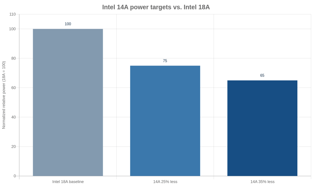
The manufacturer’s process comparison projects 15–20% higher performance at equal power, or 25–35% less power at equal performance, and up to 30% higher chip density versus Intel 18A. Intel identifies the figures as internal analysis from April 2025. They are targets for comparable designs, not independently measured results from shipping 14A processors. Combining the performance and power percentages as though measured simultaneously would misrepresent the comparison conditions.
The next tests are manufacturing and customers
Intel’s October quarterly earnings release confirms the PDK 0.9 arrived during October. Industry reporting places risk production in the second half of 2027 and a volume-production goal in 2028. Those dates remain company targets, not verified production results. Intel’s continued work with ASML on high-numerical-aperture EUV lithography illustrates the scale of process equipment preparation required beyond delivering software models.
The ecosystem includes Cadence, Synopsys, Siemens and Keysight, whose design flows and reusable intellectual-property blocks must align with the manufacturing rules. Chipmakers need credible timing, electrical characteristics and manufacturability estimates before committing expensive mask sets and verification resources. Yet a preliminary kit still leaves the practical questions of wafer defect rates, customer tape-outs, yield learning and pricing.
Next, Intel must deliver the planned PDK 1.0, disclose meaningful customer adoption and demonstrate that 14A manufacturing performance matches its projections. A design-kit milestone can advance the prospects for custom AI ASICs without establishing that a specific commercial processor has shipped.
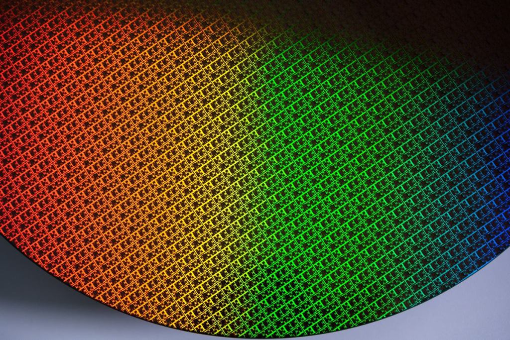
Editor’s Note. Intel 14A PDK 0.9 is design enablement, not a completed 14A chip or mass-production announcement. The performance, density and power figures are Intel’s internal projections; the chart models the stated target range. The official wafer photograph depicts older 18A technology, while the cover is a conceptual illustration.

Scan the donation code from another device if your phone cannot scan its own screen.
We volunteer daily to improve the credibility of the information on this platform. If you would like to support the research, please donate here: 3C9o19EH5HSiwEPyCTmEKzxhNCbo2X6TTb
BitcoinVersus.tech is not a financial advisor. This media platform reports on technical and financial subjects purely for informational purposes.


Leave a Reply