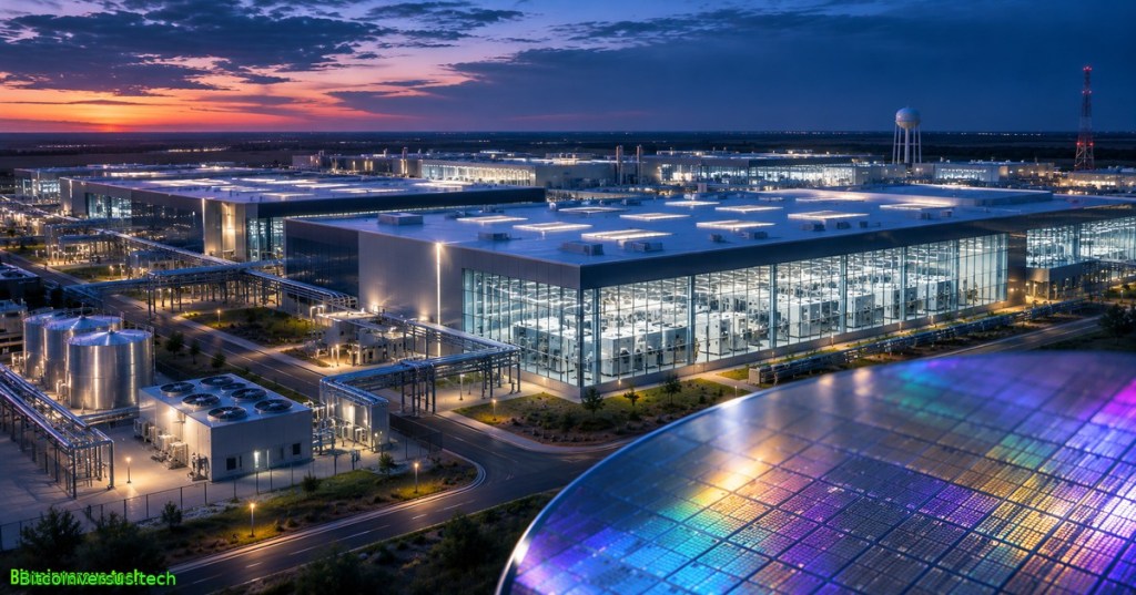
A semiconductor fabrication plant converts polished silicon wafers into circuits through repeated lithography, deposition, etching, implantation and inspection. Advanced plants also require cleanrooms, ultra-pure water, power-distribution equipment, process gases and expensive manufacturing tools. Scaling output therefore means buying and operating far more than the silicon ingots that supply the starting wafers.
On November 6, 2026, Ron Baron raised a roughly $1 trillion price tag for Elon Musk’s Terafab project. Musk described phased construction rather than an immediate outlay in their Baron Investment Conference interview. A separate Bernstein analysis, first reported in March and reiterated by Reuters in May, put the investment needed to manufacture enough AI chips for a one-terawatt annual production objective at $5 trillion–$13 trillion. Neither figure is an approved budget.
Elon Musk and Ron Baron discuss Terafab, wafer-processing efficiency and investment scale at the November 6, 2026 Baron Investment Conference. Video: Matt Pocius on Tesla Stock & Money / YouTube, rebroadcast of the conference conversation. Playback must be checked separately from embed rendering.
Why the trillion-dollar figures differ
Bernstein’s scenario concerns enough production infrastructure to deliver the desired chip output, not a purchase order for a single construction site. MarketWatch’s March 23 account describes a modeled 7 million–18 million monthly wafer starts across approximately 140–360 fabs. Matching the low and high endpoints implies roughly 50,000 wafer starts per fab per month, an arithmetic consistency check rather than a disclosed engineering specification.
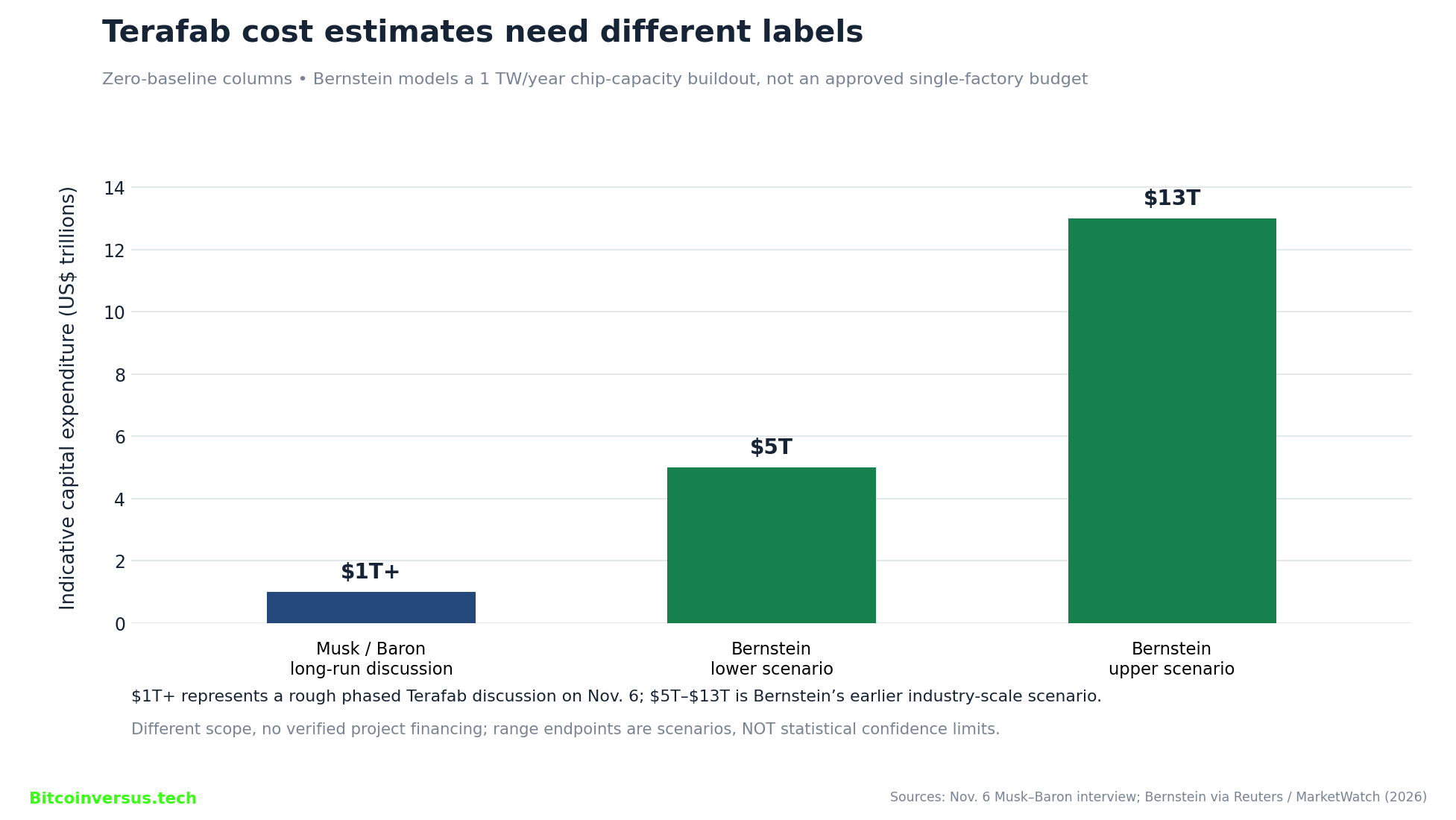
The figure also differs from actual project announcements. BitcoinVersus.Tech previously examined Texas’s more-than-$16.8 billion first-phase commitment and the proposed 2028 production timeline. Those announcements address narrower planned phases, while Bernstein extrapolates the resources needed for a much larger aspirational output level.
One terawatt of chips is not one terawatt-hour
Musk estimated global AI-chip production at 20–25 gigawatts of aggregate rated chip power in 2026 and forecast 35–45 gigawatts for 2027, versus a long-term Terafab objective of 1,000 gigawatts of chip ratings produced per year. The output goal divided by the 2027 range equals approximately 22–29 times. The figures are Musk’s estimates, not independently audited worldwide shipment totals.
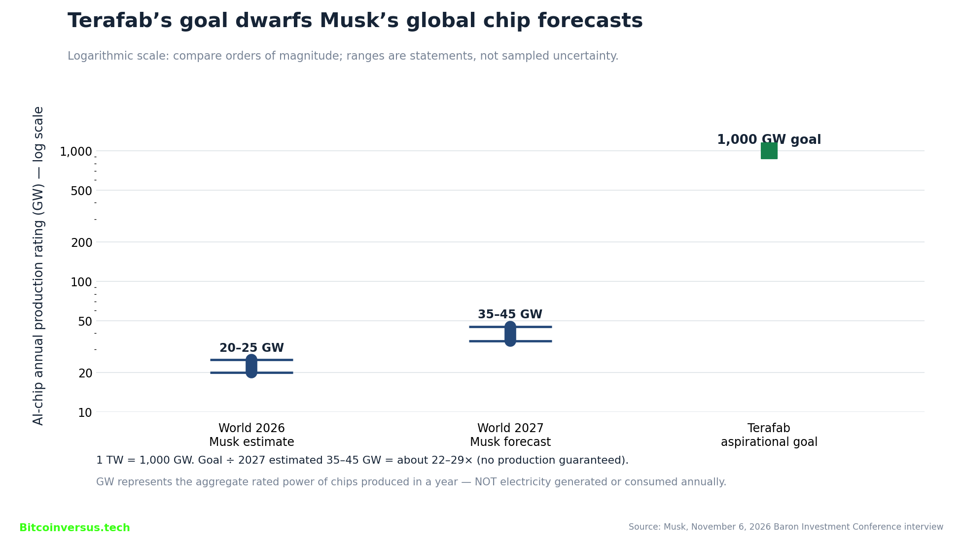
The unit distinction matters: one terawatt is a power rating, while one terawatt-hour measures energy. Adding up chips’ nameplate power ratings in an annual production cohort does not establish a factory’s instantaneous electrical demand, the chips’ actual operating consumption or their yearly energy use.
Silicon manufacturing remains the bottleneck
Tesla’s Terafab engineering recruitment describes a vertically integrated flow spanning logic, memory, packaging and lithography-mask production. Musk proposes a small Austin research fab before scaling in Grimes County. BitcoinVersus.Tech has separately covered Intel’s 14A process development and Musk’s orbital AI computing ambitions, which partly explain the demand assumptions.
Synthetic diamond is relevant mainly to packaging heat removal, not the replacement of silicon transistor wafers. The related diamond-versus-silicon engineering comparison found strong conductivity claims but no verified cost advantage in fabricating finished chips. Better heat spreading could improve packaging economics, yet cannot eliminate lithography, wafer-processing or factory-equipment investment.
What would make the forecast credible?
The open questions are financing, tool deliveries, qualified process yield, wafer starts per month, chip power per wafer and the speed of successive factory phases. A laboratory chip, a planned fab and a qualified high-volume production line represent different achievements. Bernstein’s model could prove too high if productivity improves substantially, or insufficient if yield, construction, electricity and equipment costs exceed assumptions. Without funded phases and demonstrated production, the trillions remain scenarios.
Primary sources
Musk–Baron interview transcript (November 6, 2026); Reuters Terafab factbox (May 6, 2026); MarketWatch Bernstein analysis (March 23, 2026); Tesla Terafab process-engineering job description; Texas governor’s first-phase announcement. Exact Bernstein research note was not publicly available for independent methodology review.
Editor’s Note: The $1T figure discussed by Ron Baron and Elon Musk, Bernstein’s $5T–$13T scenario and earlier Texas project commitments have distinct scopes and dates. Wafer-start and output calculations are illustrative. The 2026–27 production quantities are Musk’s estimates, not audited statistics; no financing, facility completion or video playback verification is implied. The conceptual featured cover is an original branded visualization, not a photograph of the planned Texas factory.
Support BitcoinVersus.Tech
An optional 5,000-satoshi contribution can be made by scanning the approved BitcoinVersus.Tech donation QR below with a compatible wallet. On a phone, open the article on another screen or use the wallet’s saved-image QR feature when supported. Verify the payment destination and amount before sending.

We volunteer daily to ensure the information on this platform is Verifiably True. If you would like to support the research, please scan QR code.


Leave a Reply