
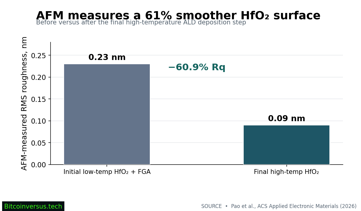
Atomic force microscopy (AFM) has revealed a 60.9% reduction in surface roughness during fabrication of an experimental gate dielectric for two-dimensional transistors. Researchers measured hafnium-oxide (HfO₂) roughness falling from 0.23 to 0.09 nanometers RMS after completing a modified atomic layer deposition process on molybdenum disulfide (MoS₂). The work appeared online on September 24, 2026, and in the October 13 issue of ACS Applied Electronic Materials. The reported improvement applies to the film surface, not chip speed or fabrication yield.
AFM scans a probe over a material to create a calibrated map of surface height. Nanoscale roughness is especially important when insulating layers cover atomically thin transistor channels, because pinholes, interface defects and uneven coverage can degrade electrical behavior. Unlike a full three-dimensional volume scan, an ordinary AFM measurement reports accessible surface topography. BitcoinVersus.Tech’s AFM reference explains the distinction between vertical sensitivity, lateral resolution and measurement uncertainty.
The 61% result comes from measured surface roughness
The team developed a deposition sequence called HALO—high-dose precursor immersion, adsorption enhancement and low-temperature oxide improvement. Initial low-temperature HfO₂ growth and forming-gas annealing produced an AFM-measured root-mean-square roughness (Rq) of 0.23 nm. After the final higher-temperature HfO₂ deposition, Rq measured 0.09 nm. The change is (0.23 − 0.09) ÷ 0.23 × 100 = 60.9%. The paper did not provide confidence intervals for the two roughness figures, so the chart does not invent error bars.
The film is an engineering achievement, but small roughness does not by itself prove a defect-free dielectric, uniform coverage across a full commercial wafer or improved transistor lifetime. Atomic layer deposition builds material through controlled surface-reaction cycles; highly inert MoS₂ surfaces make uniform initial nucleation difficult. HALO seeks to improve precursor adsorption without a separate aggressive surface-treatment step.
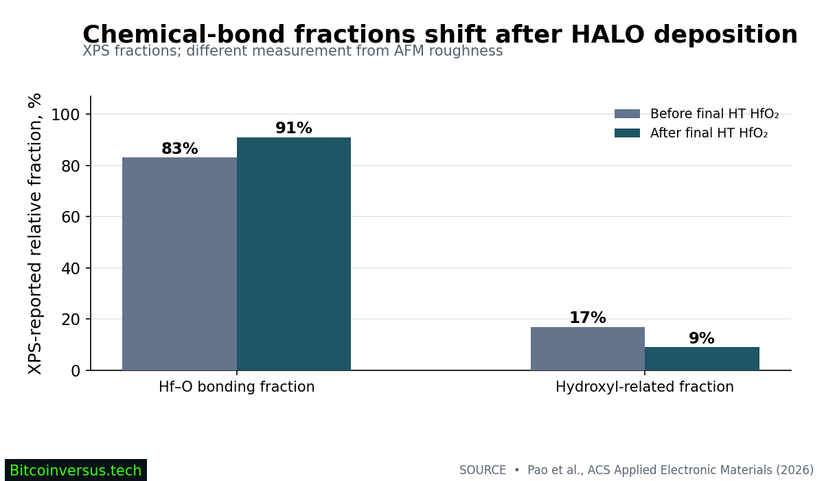
Chemical analysis tracks the improved gate stack
X-ray photoelectron spectroscopy (XPS), a separate technique from AFM, showed the fraction of Hf–O bonding increasing from 83% to 91%, while hydroxyl-related species fell from 17% to 9%. Fully oxidized HfO₂ increased from 93% to 95% in the reported chemical-state analysis. The bonding changes support improved film chemistry, but they should not be presented as direct measurements of surface height or transistor switching efficiency.
Electrical results still differ by transistor design
Optimized monolayer MoS₂ dual-gate test transistors achieved an equivalent oxide thickness (EOT) of 0.83 nm and a subthreshold swing of 80 millivolts per decade. EOT describes electrical gate-insulation equivalence to silicon dioxide, not the physical deposited film thickness or the resolution of AFM. A separate approximately 3.9-nm physical HfO₂ stack was associated with the optimized thin-dielectric result. Metal–insulator–metal test capacitors reached breakdown fields near 9 megavolts per centimeter; the capacitor figure must not be treated as a measured full-transistor breakdown rating.
The study also demonstrated conformal dielectric coverage around a nanosheet structure, but its gate-all-around device showed a much weaker subthreshold swing near 230 mV per decade. The researchers pointed to possible lithography residue and plasma-related damage. Differences between the dual-gate and gate-all-around structures mean the two switching figures are not a controlled, matched-device benchmark. The gate-all-around engineering guide explains why interface and geometry effects matter.
Other ultrathin hafnia research addresses different electrical functions and cannot be directly ranked by film thickness alone. The wafer-yield guide highlights the missing commercial evidence: sample-to-sample variability, full-wafer defect density, manufacturing throughput and qualified reliability. HALO shows promising laboratory gate-stack results, while commercial process readiness remains unproven.
Primary reference: Pao, Lin and colleagues, “Functionalization-Free Atomic Layer Deposition of Sub-1 nm EOT HfO₂ Directly on MoS₂ for Gate-All-Around Field-Effect Transistors,” ACS Applied Electronic Materials, published online September 24, 2026; October 13 issue. Technical background: NIST atomic force microscopy metrology program.
Editor’s Note: The 60.9% roughness reduction is calculated from 0.23 nm and 0.09 nm Rq values reported in the paper. AFM measured surface topography; XPS measured chemical fractions; transistor and capacitor electrical metrics came from separate test structures. EOT is electrical equivalence, not physical oxide thickness. The original paper first appeared online September 24, 2026, and in the October 13 journal issue. No independently verified wafer-scale yield, repeatability distribution or manufacturing throughput was reported. Both charts reproduce reported figures without invented uncertainty ranges. The featured image is conceptual editorial artwork, not the actual research instrument.
Support BitcoinVersus.Tech
Support independent technical journalism by scanning the original approved QR code below for an optional 5,000-satoshi donation. If reading on mobile, display the article on another screen and scan using a compatible Bitcoin wallet, or use a wallet’s supported image-scanning feature. Verify the recipient address and amount before sending funds.

We volunteer daily to ensure the information on this platform is Verifiably True. If you would like to support the research, please scan QR code.


Leave a Reply