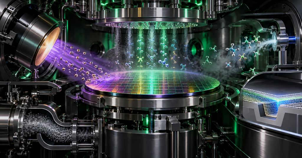
Deposition equipment builds the thin films that become conductors, dielectrics, barriers, liners, spacers, electrodes, and other critical layers inside modern semiconductor devices. Unlike etch, which removes material, deposition adds carefully controlled material to the wafer. A semiconductor technician needs to understand how vacuum, gas delivery, temperature, plasma, targets, precursors, wafer handling, chamber condition, and exhaust systems work together so that each film arrives at the correct thickness, composition, stress, and uniformity. This lesson follows OSSTC.010: Plasma Etch Equipment Basics.
Learning Objectives
- Explain the purpose of thin-film deposition in semiconductor fabrication.
- Distinguish PVD, CVD, PECVD, ALD, and PEALD at a technician level.
- Identify major deposition-tool subsystems: vacuum, gas delivery, precursor delivery, RF, heater, showerhead, sputter target, exhaust, and wafer transfer.
- Define thickness, deposition rate, conformality, step coverage, uniformity, film stress, and chamber matching.
- Recognize common symptom patterns without casually changing a qualified process recipe.
- Build a safe first-line troubleshooting sequence that preserves data before resets or maintenance.
PVD: Moving Material From a Solid Target to the Wafer
Physical vapor deposition, or PVD, commonly uses sputtering. A high-vacuum chamber contains a high-purity target made from the material that will become the film. A plasma—often using argon—accelerates ions toward that target. The impact ejects target atoms, and those atoms travel through the chamber and condense on the wafer. PVD is widely used for conductive and barrier films because it can deposit metals cleanly and at high throughput. For technicians, the critical signals include base pressure, process pressure, target condition, DC or RF power, reflected power where applicable, gas flow, wafer temperature, deposition rate, and target lifetime.
CVD and PECVD: Building Films From Reactive Gases
Chemical vapor deposition, or CVD, forms a solid film through controlled chemical reactions involving gaseous precursors at the wafer surface. Thermal CVD relies mainly on temperature to drive those reactions, while plasma-enhanced CVD, or PECVD, uses plasma energy so useful films can often be deposited at lower wafer temperatures. A production CVD tool therefore behaves like a vacuum reactor, gas-delivery system, thermal system, and sometimes an RF-plasma system at the same time. The technician watches precursor availability, MFC command versus actual flow, chamber pressure, heater or chuck temperature, RF status, exhaust performance, showerhead condition, and chamber-clean state.
ALD and PEALD: Thickness Control One Reaction Cycle at a Time
Atomic layer deposition, or ALD, separates surface reactions into a repeating sequence of precursor pulse, purge, reactant pulse, and purge. Because each surface reaction is self-limiting, ALD can produce highly conformal films over complex three-dimensional structures with extremely precise thickness control. Plasma-enhanced ALD, or PEALD, adds plasma to provide reaction energy and can reduce the thermal budget for some films. Technician attention shifts toward pulse timing, purge effectiveness, precursor delivery stability, chamber temperature, line temperature, valve response, plasma ignition for PEALD, and chamber-to-chamber matching.
What Is Inside a Deposition Tool
- Load ports and wafer transfer: move wafers through atmospheric and vacuum environments while preserving orientation and cleanliness.
- Process chamber: contains the wafer and creates the controlled environment for film formation.
- Vacuum system: roughing pumps, turbomolecular or other process pumps, throttle valves, forelines, pressure gauges, and isolation valves.
- Gas delivery: facility gases, gas cabinets, regulators, MFCs, valves, purge lines, and distribution plumbing.
- Precursor delivery: bubblers, ampoules, heated lines, vapor draw systems, direct-liquid injection, or other chemistry-specific delivery hardware.
- Energy source: substrate heaters, RF plasma sources, DC sputter power, RF sputter power, or remote plasma depending on process type.
- Distribution hardware: showerheads, injectors, gas rings, or source geometry that controls material delivery across the wafer.
- Exhaust and abatement: removes unreacted chemistry and reaction byproducts safely.
- Control system: recipes, interlocks, chamber qualification, calibration records, alarms, trace data, and maintenance counters.
The Numbers Technicians Watch
- Film thickness: how much material was deposited.
- Deposition rate: film thickness added per unit time or per ALD cycle.
- Uniformity: thickness or film-property variation across the wafer.
- Conformality: how evenly a film coats three-dimensional surfaces.
- Step coverage: how well sidewalls and bottoms of features are coated relative to top surfaces.
- Film stress: tensile or compressive mechanical stress that can affect wafer bow, adhesion, cracking, and device performance.
- Sheet resistance or resistivity: critical electrical metrics for conductive films.
- Refractive index or composition: common indicators for dielectric or compound films.
- Particle count: a major contamination and yield indicator.
- Chamber matching: the ability of different chambers to produce equivalent wafer results.
Common Symptom Patterns
- Low deposition rate: check precursor level, gas flow, source delivery, pressure, temperature, power, target age, valve timing, and chamber condition.
- High deposition rate: verify recipe, MFC calibration, pressure control, source output, temperature, and timing.
- Center-to-edge nonuniformity: inspect showerhead or source condition, wafer centering, heater/chuck behavior, gas distribution, pressure, chamber deposits, and target erosion pattern.
- Poor conformality: confirm process mode, pulse/purge timing, precursor transport, pressure, temperature, and whether the correct chamber and recipe were used.
- Particles rising: review chamber deposits, flaking, shield condition, hardware wear, transfer cleanliness, recent maintenance, and seasoning history.
- High film stress: compare pressure, temperature, RF power, gas ratio, deposition rate, chamber condition, and recent hardware changes.
- Plasma will not ignite: verify gas availability, pressure window, RF enable, match state, grounding, interlocks, and chamber readiness.
- Precursor delivery unstable: inspect source temperature, line temperature, carrier gas, pressure, level indication, valve actuation, and delivery-line condition.
- Vacuum recovery slow: check chamber seals, valve state, pump condition, foreline pressure, deposits, and possible leaks.
Safe First-Line Troubleshooting
- Confirm tool, chamber, recipe, lot, wafer, layer, and exact alarm text.
- Capture timestamps, screenshots, pressure traces, gas or precursor flows, temperatures, RF or DC power, vacuum state, and maintenance counters before resetting.
- Determine whether the problem affects one wafer, one lot, one chamber, or the whole platform.
- Check facility gases, precursor source status, CDA, cooling water, exhaust, vacuum, RF/DC power, heaters, and wafer-transfer readiness.
- Compare actual values against qualified normal ranges and a recent known-good wafer.
- Review recent chamber cleans, target changes, kit changes, source bottle changes, PM work, calibrations, and seasoning cycles.
- Run only approved recoveries, cleans, seasoning, calibrations, or qualification procedures.
- Do not bypass interlocks or change qualified recipe values just to make a fault disappear.
- Escalate with preserved traces, lot history, chamber count, maintenance history, and checks already completed.
Technician Fault Map
| Symptom | First Systems to Check |
|---|---|
| No film or very low thickness | Recipe, source/precursor, MFCs, pressure, heater, RF/DC power, target condition, chamber readiness |
| Nonuniform film | Showerhead/source geometry, wafer centering, heater/chuck, gas distribution, pressure, chamber deposits |
| Particle excursion | Shields, chamber wall deposits, flaking, transfer path, PM history, seasoning |
| High resistance metal film | Thickness, composition, contamination, target/source condition, pressure, power, temperature |
| ALD cycle drift | Pulse timing, purge timing, precursor delivery, valve response, temperature, pressure |
| PECVD plasma instability | RF power, match state, gas flow, pressure, chamber condition, grounding |
| Slow pumpdown | Door/seal integrity, valves, pump state, foreline, chamber deposits, leak indicators |
Hands-On Exercise
- Draw one simplified PVD chamber and label the target, plasma, wafer, gas inlet, pressure control, and vacuum pump.
- Draw one simplified CVD or PECVD chamber and label the precursor/gas source, showerhead, wafer heater, pressure control, RF source if present, and exhaust.
- Write the four-step ALD sequence: precursor pulse, purge, reactant pulse, purge.
- Create a troubleshooting table for three cases: low deposition rate, center-to-edge nonuniformity, and a particle excursion.
- For each case, list the data you would capture before any reset, recipe edit, chamber opening, or maintenance action.
Knowledge Check
- What is the main purpose of deposition in semiconductor fabrication?
- What physical mechanism is commonly used in PVD?
- How does CVD differ from PVD?
- What does PECVD add to a CVD process?
- Why is ALD highly conformal?
- What is step coverage?
- Name four tool systems that can cause deposition-rate drift.
- Why can chamber condition affect film results?
- What should a technician capture before resetting an intermittent deposition fault?
- Why should qualified deposition recipe values not be changed casually during troubleshooting?
Answers
- To add precisely controlled conductive, dielectric, barrier, liner, spacer, electrode, or other material layers to the wafer.
- Sputtering, where plasma ions eject atoms from a solid target.
- CVD forms a film through chemical reactions involving gaseous precursors; PVD physically transfers material from a source or target.
- Plasma energy, which can activate reactions and often reduce the required wafer temperature.
- Its surface reactions are sequential and self-limiting, allowing controlled coating of complex topography.
- The ability of a process to coat sidewalls and feature bottoms relative to top surfaces.
- Examples include source/precursor delivery, MFCs, pressure control, temperature, RF/DC power, target condition, and chamber condition.
- Deposits, wall coatings, target erosion, seasoning, contamination, and hardware wear can change gas flow, plasma behavior, surface chemistry, particles, and heat transfer.
- Alarm text, timestamps, screenshots, pressure, gas/precursor data, temperature, power, vacuum state, wafer/lot identity, chamber identity, and recent maintenance history.
- Changing qualified values can mask the real fault, create additional variation, damage wafers, and invalidate comparison against known-good production behavior.
Previous Related Lessons
- OSSTC.010: Plasma Etch Equipment Basics
- OSSTC.006: Semiconductor RF Power Delivery
- OSSTC.003: Semiconductor Vacuum Systems
Primary References
- Applied Materials — Materials Deposition: overview of PVD, CVD, ALD, selective deposition, and film-control variables.
- ASM — Atomic Layer Deposition: ALD and PEALD fundamentals, pulse-and-purge cycles, conformality, and production tools.
- SK hynix — Front-End Process: Deposition: practical comparison of CVD and PVD in wafer fabrication.
Rotation next: Semiconductor Engineer.
BitcoinVersus.Tech Editor’s Note:
We volunteer daily to ensure the credibility of the information on this platform is Verifiably True. If you would like to support to help further secure the integrity of our research initiatives, please donate using the QR code provided

For best QR-code scanning results, please scan this donation code from a desktop or larger screen. Mobile screens may prevent camera recognition.
BitcoinVersus.Tech provides technical education and analysis for informational purposes only.


Leave a Reply