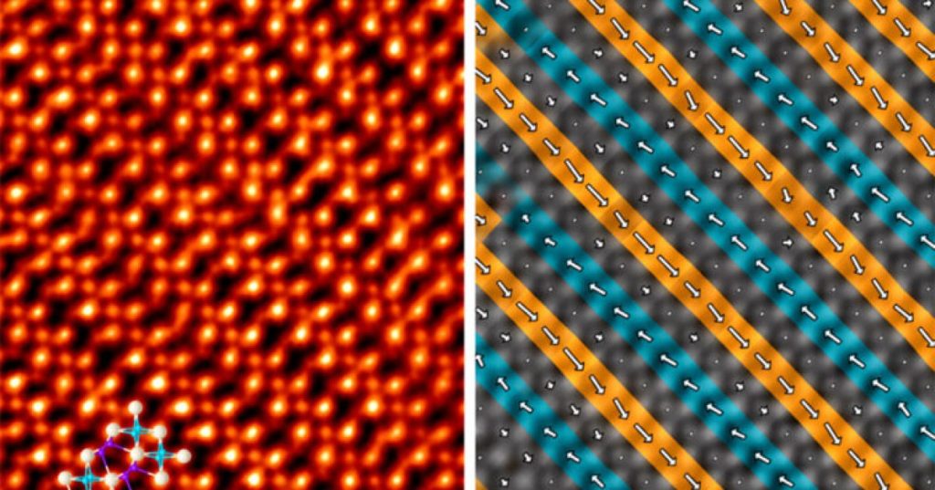
Researchers at Washington University in St. Louis and the University of Nebraska–Lincoln have identified a way to preserve an electrically switchable structure in ultrathin hafnium oxide, an established semiconductor material. Washington University’s November 5 research report highlights experiments demonstrating antiferroelectric order in lanthanum-doped hafnia films as thin as 0.6 nanometers. The underlying peer-reviewed Science study was published September 24, 2026; the November update explains its implications rather than announcing a newly shipped memory product.
What antiferroelectricity means for a semiconductor
Hafnium oxide, written HfO₂, already serves as a high-permittivity insulating material in modern transistors. A ferroelectric material retains a preferred electrical polarization after an external field is removed. An antiferroelectric has neighboring dipoles oriented in opposing directions, producing little net polarization until a sufficiently strong electric field drives a phase transition. The field-dependent behavior can be exploited for energy-storage capacitors and, potentially, new memory-device structures.
The Nebraska-led team grew highly ordered single-crystal films of lanthanum-doped hafnia on yttria-stabilized zirconia substrates. Compressive strain at the interface helped stabilize an orthorhombic structure with antiparallel polarization. Instead of fading as the film became thinner, the antiferroelectric ordering persisted down to roughly one unit cell, near 0.6 nm. Nebraska’s experimental summary reports stability to 850°C under the study’s conditions; that temperature is a material observation, not an operating rating for a finished processor or memory module.
Microscopy and modeling agree at atomic scale
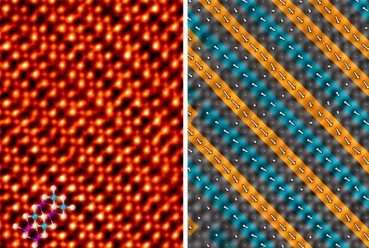
Rohan Mishra’s group at WashU used advanced scanning transmission electron microscopy to resolve atomic-column arrangements and map the displacement of oxygen atoms. Xiaoshan Xu and colleagues synthesized the films, while Alexei Gruverman’s group used electrical measurements to identify the characteristic double-hysteresis response. Quantum-mechanical calculations provided a separate test of whether the observed structure could be energetically stable. A combination of imaging, electrical behavior and theory helps distinguish intrinsic antiferroelectricity from apparent switching produced by trapped charges.

The measurements build on a broader effort to understand materials through semiconductor lattice physics and nanoscale imaging. BitcoinVersus.Tech previously explained semiconductor metrology and inspection, techniques that are essential when electrical behavior depends on the position of only a few atoms.
Potential for memory, capacitors and lower-energy devices
Antiferroelectric films could be useful where charge must be stored and released rapidly, although the research has not established commercial endurance, read/write performance, array yield or manufacturing cost. The new experimental geometry uses controlled single crystals and a selected substrate; scaling to large wafers and integrating electrodes without disturbing the desired phase are separate engineering tasks.
Another Advanced Materials study first published October 21, involving Mishra and collaborators, observed sub-square-nanometer ferroelectric domains in zirconia, a related oxide. Predicted conductive domain walls could eventually support compact electronic functions, but the calculations do not establish a working nanoscale memory chip. Both investigations concern material properties rather than available commercial storage.

Potential applications would compete against established silicon and emerging nonvolatile-memory designs. Earlier BitcoinVersus.Tech articles outlined memory architectures and their performance trade-offs and examined new semiconductor design infrastructure. Commercial adoption will require reproducible switching, defect control, compatibility with fabrication steps, and reliable lifetime measurements. The verified finding is atomic-scale order under carefully designed experimental conditions—not a forecast of near-term memory capacity or energy savings.
Editor’s Note: Findings, material composition and researcher roles were checked against Washington University’s November 5, 2026 report, Nebraska’s September 28 research summary, the September 24 Science article (DOI: 10.1126/science.ady5526) and the October 21 Advanced Materials paper (DOI: 10.1002/adma.75144). The two research projects are distinct. Atomic-scale order and predicted future applications must not be confused with a commercial memory demonstration. The cover uses authentic microscopy from the Mishra laboratory, resized for editorial display; researcher photographs are university-supplied. No unrelated video was embedded as a substitute for verified topic-specific footage.

To donate 5,000 sats, open the article on a separate display and scan the original QR code with a compatible Bitcoin wallet. On mobile, use another screen or your wallet’s supported image-scanning feature. Verify the destination 3C9o19EH5HSiwEPyCTmEKzxhNCbo2X6TTb before sending.
We volunteer daily to ensure the information on this platform is Verifiably True. If you would like to support the research, please scan QR code.
BitcoinVersus.tech is not a financial advisor. Scientific and semiconductor coverage is provided for informational purposes.


Leave a Reply