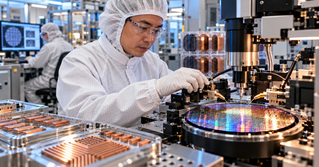
Backside power delivery moves a chip’s power-distribution wiring to the opposite side of the wafer from its main signal interconnects. OSSEC.011 follows OSSEC.010 on CFET stacking, but studies a separate engineering problem: getting a stable supply voltage to densely packed transistors. Intel’s PowerVia explanation shows how separating power from signal routing can shorten the power path and relieve frontside congestion. The goal is better delivery, not a new source of electricity.
Key Takeaways
- Backside power delivery changes the wiring architecture; it is not the same as gate-all-around channels or CFET transistor stacking.
- Resistive voltage drop follows ΔV = I × R. Lower path resistance can preserve more voltage at the load.
- Buried power rails and nano-through-silicon vias are one implementation, not a universal recipe.
- A useful comparison includes power integrity, routing, contacts, thermal behavior, manufacturability, and reliability.
Elementary Overview
Think of signal wires as messages and power wires as the supply routes that let the receivers work. Sharing the frontside metal stack makes both networks compete for space. Imec’s process overview explains how wider, less resistive backside routes can feed the devices through vertical connections. The basic electrical principle is the same as Ohm’s law: current flowing through resistance causes a voltage drop. Real chip power grids are distributed networks, so this simple model is a starting point, not a full signoff simulation.
Follow the Power Path
- Conventional frontside path: supply connections feed a frontside metal-and-via network, which reaches local rails and transistor terminals.
- One backside implementation: backside metal feeds nano-through-silicon vias, then buried power rails and device contacts. Other schemes use different backside contacts; imec’s comparison explains why connectivity choices matter.
- Manufacturing sequence: in imec’s illustrated buried-rail flow, frontside fabrication is followed by carrier bonding, wafer thinning, backside via formation, and backside metallization. Exact materials and dimensions depend on the process.
- Keep the boundaries clear: GAA electrostatics concerns gate control of the channel; CFET stacks complementary transistors; backside power changes how supply and return connections reach them.
Worked IR-Drop Example
- Assumptions: an illustrative local circuit draws 0.20 A from a 0.70 V source. The effective resistance of its supply-and-return path is 0.10 Ω. These are teaching values, not measurements of a commercial process.
- Original path: ΔV = 0.20 A × 0.10 Ω = 0.020 V = 20 mV. The available local supply difference is approximately 0.680 V.
- Lower-resistance path: at the same current, 0.04 Ω gives ΔV = 8 mV and approximately 0.692 V at the load.
- Interpretation: the modeled resistive drop falls by (20 − 8) ÷ 20 = 60%. That is not a 60% reduction in total chip energy, temperature, or execution time.
- Model limit: fast current changes also involve inductance and decoupling. Timing, workload, and spatially varying current must be included in a real power-integrity analysis.
What an Engineer Must Check
- Electrical access: extract the complete rail, via, interface, and contact resistance. A short route is not automatically a low-resistance route.
- Dynamic behavior: compare worst-case local voltage across switching activity, process, voltage, and temperature conditions—not only average DC drop.
- Integration: inspect wafer-thinning uniformity, backside alignment, isolation, and metal continuity. Check thermal behavior and long-term current-density limits.
- Design closure: compare routed area, timing, and power with equivalent circuit assumptions. Siemens’ extraction discussion highlights the need to model both sides of the structure.
- System boundary: die-level supply routing is only one part of semiconductor packaging and assembly. It does not eliminate package losses, voltage regulation, or cooling.
Practice
- Sketch separate paths for a logic signal, VDD supply, and VSS return. Mark the transistor layer and the two wafer faces.
- Repeat the worked calculation at 0.40 A while keeping both resistance values unchanged.
- Calculate I²R loss for each original 0.20 A path. Explain why this is path loss rather than total chip power.
- Write a comparison plan that holds workload and operating conditions constant while checking local voltage, timing, temperature, and yield.
Knowledge Check
- Does backside power delivery require CFET stacking?
- Why can lower-resistance delivery improve the voltage available to a load?
- What are the new drops at 0.40 A for 0.10 Ω and 0.04 Ω?
- What are the path losses at 0.20 A?
- Why is an IR-drop percentage not a complete chip-efficiency result?
Answers
- No. The power-routing architecture and transistor-stacking architecture address different problems.
- With current held constant, ΔV = I × R decreases as path resistance decreases.
- 40 mV and 16 mV, respectively.
- 4 mW and 1.6 mW, using P = I²R.
- Total behavior also depends on device switching and leakage, workload, timing, regulation, packaging, thermal conditions, and other losses.
Elementary Conclusion
Backside power delivery gives the power network its own physical routing space and can reduce the resistance between a supply and the active devices. The useful habit is to follow the complete current loop, calculate the voltage actually available at the load, and then test the full design. A smaller modeled IR drop is meaningful evidence about that power path; it becomes a product-level benefit only after the surrounding circuit and manufacturing constraints are evaluated.
Sources and Further Reading
- Intel: PowerVia manufacturing and test-chip explanation — primary source, June 5, 2023.
- imec: Backside power delivery — buried-rail process flow and integration tradeoffs.
- imec: A DTCO study of backside connectivity options.
- Siemens EDA: CFET and backside-power extraction challenges — September 30, 2026.
BitcoinVersus.Tech Editor’s Note:
We volunteer daily to ensure the credibility of the information on this platform is Verifiably True. If you would like to support to help further secure the integrity of our research initiatives, please donate using the QR code provided

For best QR-code scanning results, please scan this donation code from a desktop or larger screen. Mobile screens may prevent camera recognition.


Leave a Reply