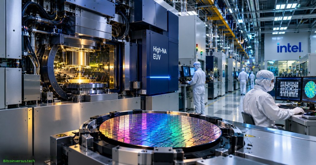
An Intel executive has identified a physical ceiling on the AI chip industry’s near-term growth. In an October 22, 2026, factory-tour interview, Intel Chief Technology Officer Pushkar Ranade estimated the existing global inventory of advanced chipmaking equipment could support roughly twice current leading-edge wafer output—but not ten times as much. The distinction matters as foundries race to translate soaring demand for AI accelerators into actual silicon shipments.
Dwarkesh Patel, “What will computer chips look like in 2045?” published October 22, 2026. Intel’s factory-development discussion begins at 00:47; the equipment-capacity exchange begins at 48:00. Original interview and fab tour. Credit: Dwarkesh Podcast / YouTube.
A supply chain cannot expand by capital alone
Advanced logic chips begin as silicon wafers that pass through thousands of deposition, etching, cleaning, inspection and lithography operations. Each tool family has its own delivery lead times, qualified consumables and production constraints. Asked whether the world’s available equipment could support tenfold leading-edge wafer output, Ranade replied, “Not 10X, but probably 2X, yes.” The figure is an executive estimate, not a measured global capacity audit or forecast of completed production.
Patel noted that AI computing capacity has historically risen rapidly, but demand for compute is not equivalent to wafer starts. Chips can improve through architecture, packaging and efficiency without matching increases in wafer volume. Even fully financed cleanroom expansions would need scanners, process chambers, skilled operators, power, water and qualified materials. Earlier ASML supply-demand coverage outlined the same upstream constraint from a different angle.
Why EUV scanners are difficult to replace
Extreme ultraviolet lithography projects intricate circuit patterns using 13.5-nanometer light. High-numerical-aperture EUV uses more capable optics that can reduce multiple patterning exposures on selected layers, potentially improving process simplicity and yield. High-NA also introduces substantial equipment, mask and integration costs; no single tool upgrade multiplies total fab output by the same factor.
ASML, “Inside the machine: How a High NA system generates EUV light,” August 21, 2025. Greet Storms explains the tin-droplet plasma light source. Official manufacturer demonstration, not an independent throughput test. Credit: ASML / YouTube.
In September, Intel and ASML reported more than one million wafers processed across High-NA tool certification, research, testing and production, including select layers on a subset of Panther Lake processors. The cumulative total is not one million saleable finished chips or proof that all wafers were volume-production wafers. The result extends BitcoinVersus.Tech’s High-NA production report and its photomask-format analysis.
Intel 14A shows the gap between development and capacity
In the tour, process leader Chris Auth described roughly 2,000 fabrication steps, with inline metrology and electrical tests locating defects before engineers analyze cross-sections and adjust recipes. Intel’s November 2 update said its 14A process design kit had reached version 0.9, providing silicon-validated models and design rules for external customers. Intel expects PDK 1.0 in the first quarter of 2027; a design-kit milestone does not mean 14A has entered high-volume manufacturing. The site’s earlier 14A PDK report covers the release in detail.
ASML, “Why is the wafer stage important in High NA EUV lithography?” October 2, 2025. Official explanation of precise wafer handling, alignment and scanning. Background footage, not Intel’s October 2026 fab tour. Credit: ASML / YouTube.
The next bottlenecks reach beyond transistors
Gate-all-around transistors improve electrostatic control, backside power routes electrical supply separately from signal wiring, and hybrid bonding creates dense vertical connections between dies. Each improvement requires yield learning and new integration steps. Earlier gate-all-around engineering lessons and hybrid-bonding coverage explain the mechanisms.
Ranade also discussed rethinking cleanroom economics and fab layouts, but offered no demonstrated alternative able to replace contamination-controlled manufacturing. A hypothetical Terafab or other mega-project would face the same equipment ecosystem. The central question is how much more useful compute can be delivered per wafer while equipment suppliers expand—not whether a speculative factory alone can eliminate shortages.
Primary sources: Dwarkesh Patel’s October 22 interview and full transcript; Intel’s November 2 14A design-kit update; Intel–ASML September 7 High-NA milestone; ASML scanner specifications.
BitcoinVersus.Tech Editor’s Note
Published November 8, 2026. The twofold estimate comes from Intel CTO Pushkar Ranade’s October 22 interview and represents his judgment regarding the existing global tool inventory, not a verified equipment count or prediction of future wafer shipments. Intel’s September High-NA wafer total includes test, research and selected production use. The 14A PDK update does not establish mass production. The featured Intel cleanroom scene is original conceptual artwork, not an authentic photograph or exact machine model. ASML demonstrations are older official technical explainers.
We volunteer daily to ensure the information on this platform is Verifiably True. If you would like to support the research, please scan QR code.

To make an optional 5,000-satoshi contribution, scan the original QR with a Bitcoin wallet using a second screen. Mobile readers can save the image and use a compatible wallet’s image-scanning feature. Before sending, verify destination 3C9o19EH5HSiwEPyCTmEKzxhNCbo2X6TTb and the amount displayed by the wallet.
BitcoinVersus.Tech reports manufacturing and financial developments for informational purposes, not as investment advice.


Leave a Reply